
Electron Microscope
Filter
Showing 181–210 of 532 results
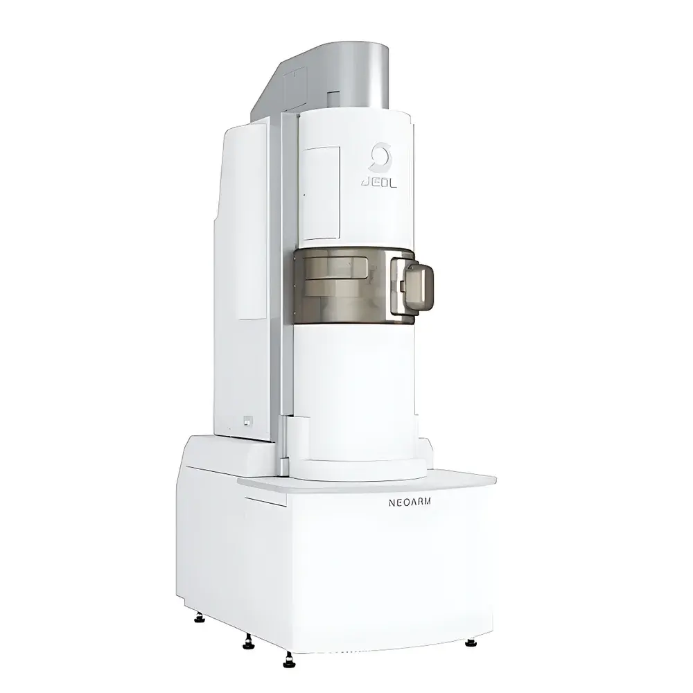
| Brand | JEOL |
|---|---|
| Origin | Japan |
| Model | JEM-ARM200F(C)-NEO ARM |
| Acceleration Voltages | 30 kV, 80 kV, 200 kV |
| Magnification Range | 50× to 2,000,000× |
| Point Resolution | 0.078 nm (at 200 kV) |
| Energy Resolution | ≤0.3 eV (with monochromated cold FEG) |
| Configuration | Dual spherical aberration correctors (objective and condenser), integrated STEM/TEM/EELS/EDS platform |
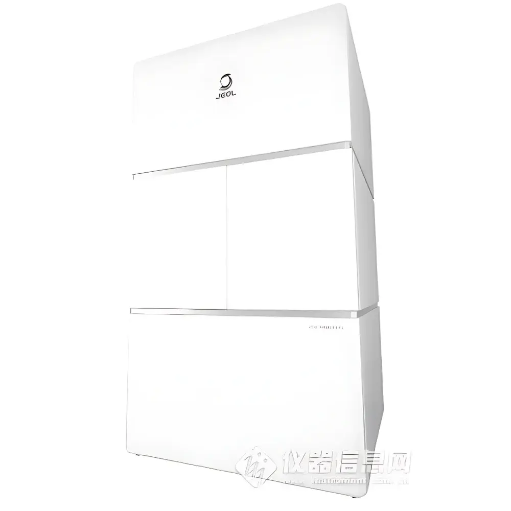
| Brand | JEOL |
|---|---|
| Origin | Japan |
| Manufacturer Type | Authorized Distributor |
| Product Origin | Imported |
| Model | JEM-ARM300F2 |
| Price | USD 6.8M (est.) |
| Acceleration Voltage | Up to 300 kV |
| Magnification Range | 100×–2,000,000× |
| Guaranteed HAADF-STEM Resolution | 53 pm (300 kV, with ETA corrector + FHP2 polepiece) |
| EDS Detector | Dual large-area SDD (158 mm² total active area) |
| Solid Angle for EDS | 2.2 sr (with WGP polepiece) |
| Cs Corrector | JEOL 12-Pole Monochromator-Based Spherical Aberration (Cs) Corrector |
| Software | COSMO™ Auto-Aberration Correction Suite |
| Gun Type | Next-Generation Cold Field-Emission Gun (Cold-FEG) |
| Environmental Shielding | Integrated Active Vibration & Acoustic Damping Enclosure |
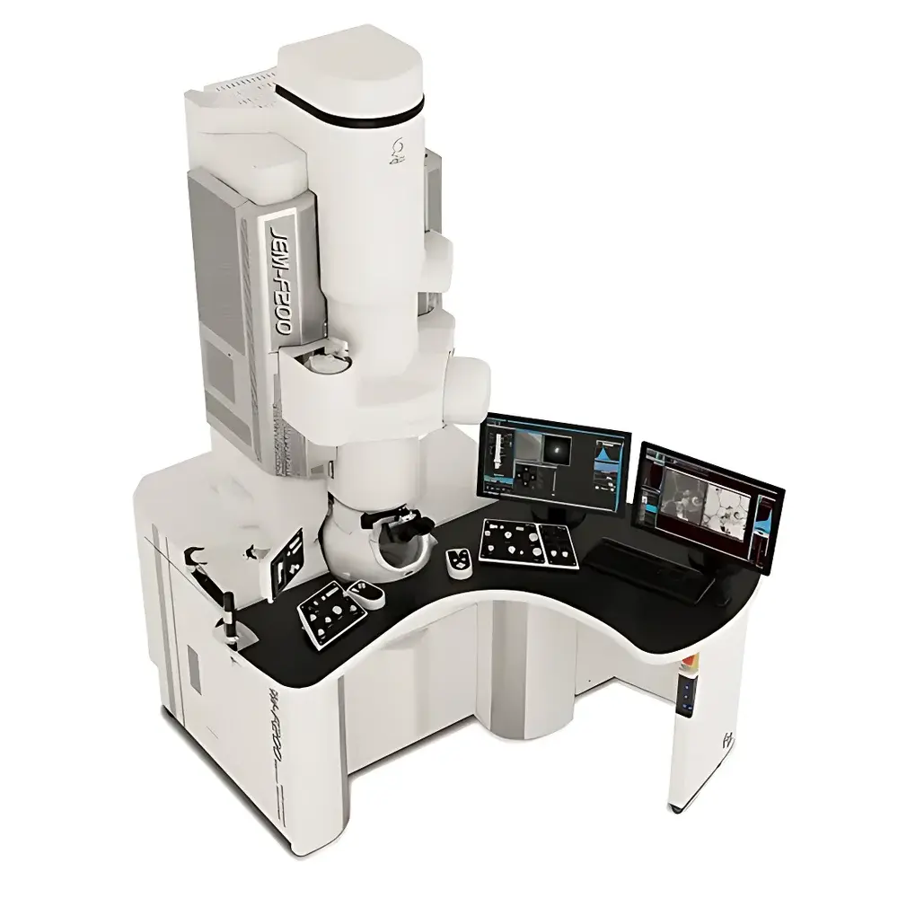
| Brand | JEOL |
|---|---|
| Origin | Japan |
| Model | JEM-F200 |
| Price | USD $2,000,000 |
| Acceleration Voltage | Up to 200 kV |
| Magnification Range | 50× – 2,000,000× |
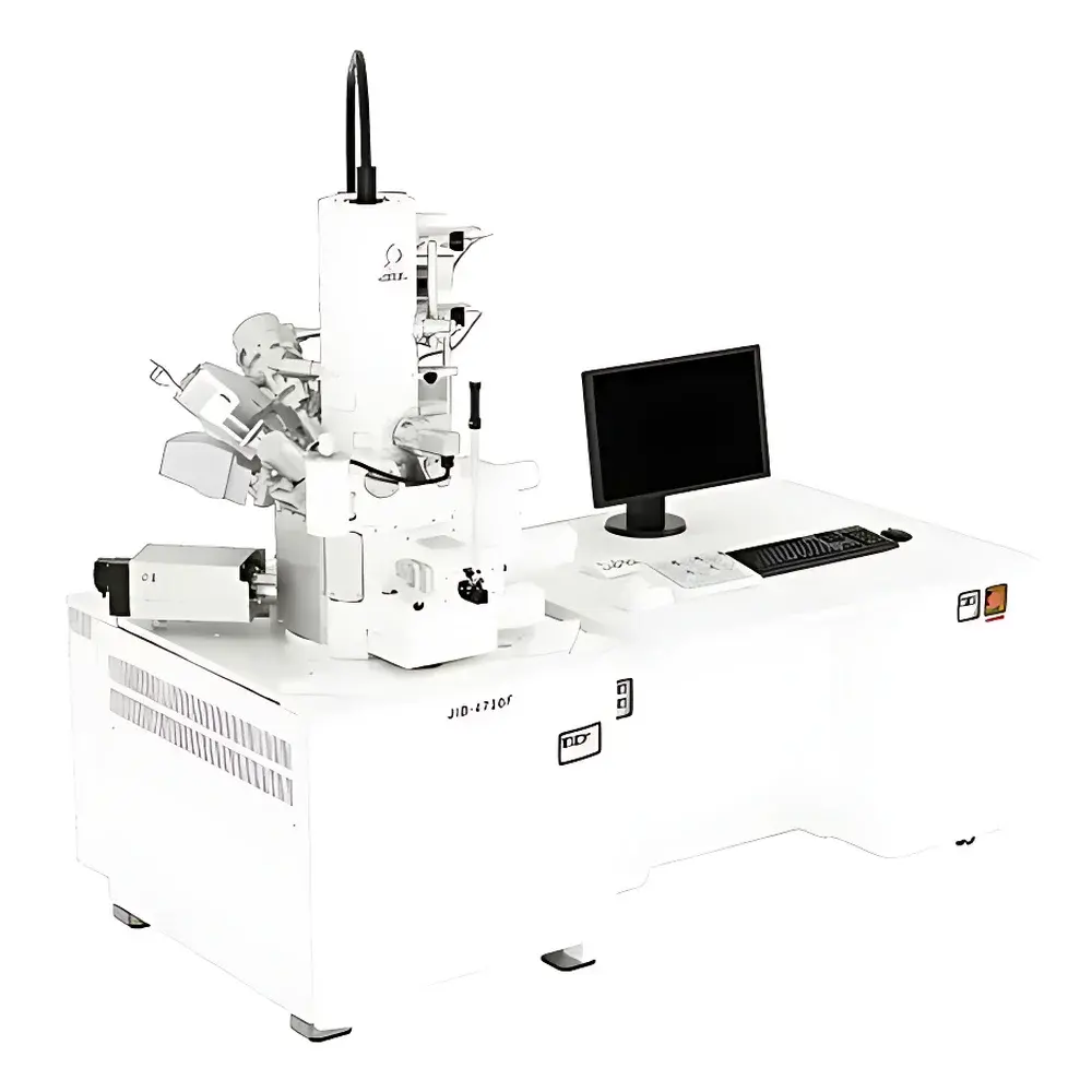
| Brand | JEOL |
|---|---|
| Origin | Japan |
| Model | JIB-4700F |
| Instrument Type | Benchtop Dual-Beam FIB-SEM |
| Electron Source | Cold Field Emission Gun (CFEG) |
| Secondary Electron Resolution | 1.2 nm @ 15 kV, 1.6 nm @ 1 kV |
| Backscattered Electron Resolution | 2.5 nm |
| FIB Resolution | 5 nm @ 30 kV |
| Magnification Range | 25× – 1,000,000× |
| Acceleration Voltage | 0.1–30 kV |
| Maximum FIB Current | 90 nA |
| Maximum SEM Probe Current | 300 nA |
| Gas Injection System | Up to 3 independent channels |
| Sample Stage | 5-axis fully aligned motorized stage |
| Maximum Sample Diameter | 150 mm |
| Sample Loading | Airlock-style exchange |
| Detector Interfaces | EDS, EBSD, STEM, SE/BSE |
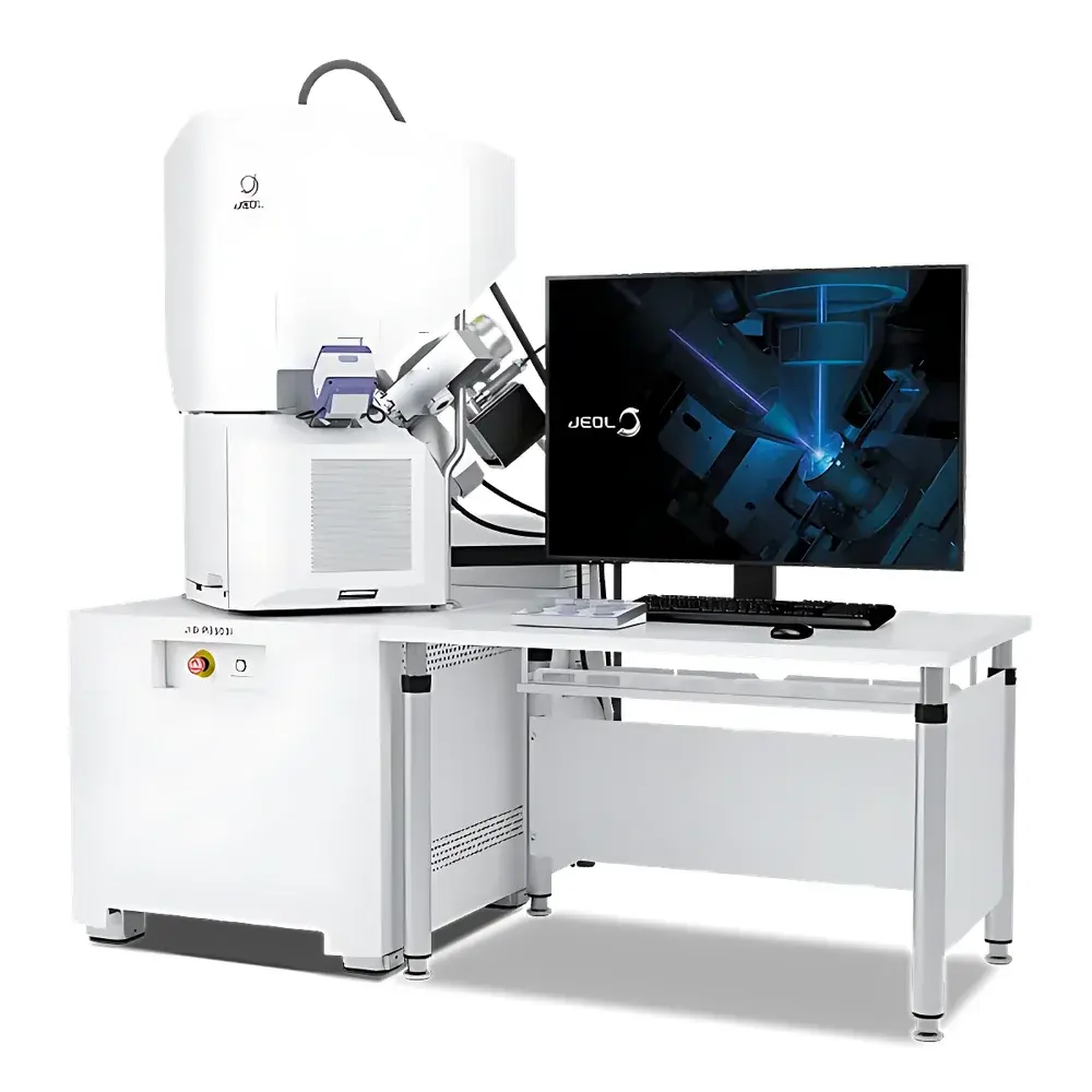
| Brand | JEOL |
|---|---|
| Origin | Japan |
| Model | JIB-PS500i |
| Electron Beam Resolution | 0.7 nm @ 15 kV, 1.0 nm @ 1 kV |
| Ion Beam Resolution | 3 nm |
| Maximum Ion Beam Current | 100 nA |
| Maximum Electron Beam Current | 500 nA |
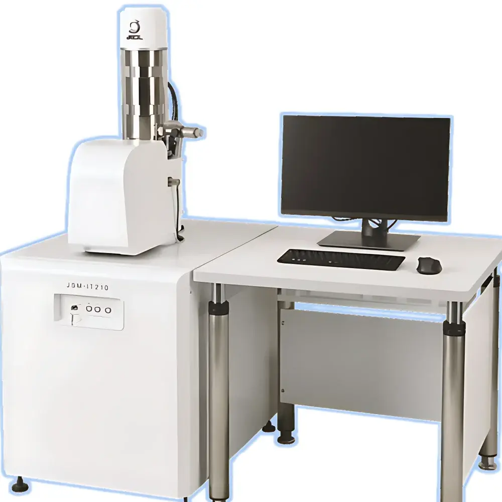
| Brand | JEOL |
|---|---|
| Origin | Japan |
| Model | JSM-IT210 |
| Instrument Type | Floor-standing |
| Electron Source | Tungsten Filament |
| Secondary Electron Resolution | 3 nm @ 30 kV |
| Magnification Range | 5× – 300,000× |
| Accelerating Voltage | 0.5–30 kV |
| Backscattered Electron Resolution | 4 nm (Low Vacuum Mode) |
| Maximum Sample Dimensions | Ø150 mm × 53 mm height |
| Specimen Chamber Expansion Ports | Multiple |
| Stage Type | Motorized 5-Axis Stage |
| Standard Detectors | Everhart-Thornley SE Detector, Solid-State BSE Detector |
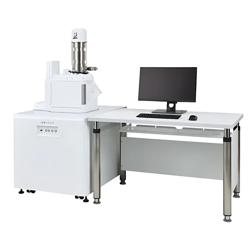
| Brand | JEOL |
|---|---|
| Origin | Japan |
| Model | JSM-IT510 |
| Instrument Type | Floor-standing SEM |
| Electron Source | Tungsten Filament |
| Secondary Electron Resolution | 3 nm @ 30 kV, 15 nm @ 1 kV |
| Backscattered Electron Resolution | 4 nm @ 30 kV |
| Accelerating Voltage Range | 0.3–30 kV |
| Magnification Range | 14×–800,000× (on display) |
| Vacuum Mode | Low-vacuum compatible with LHSED detector |
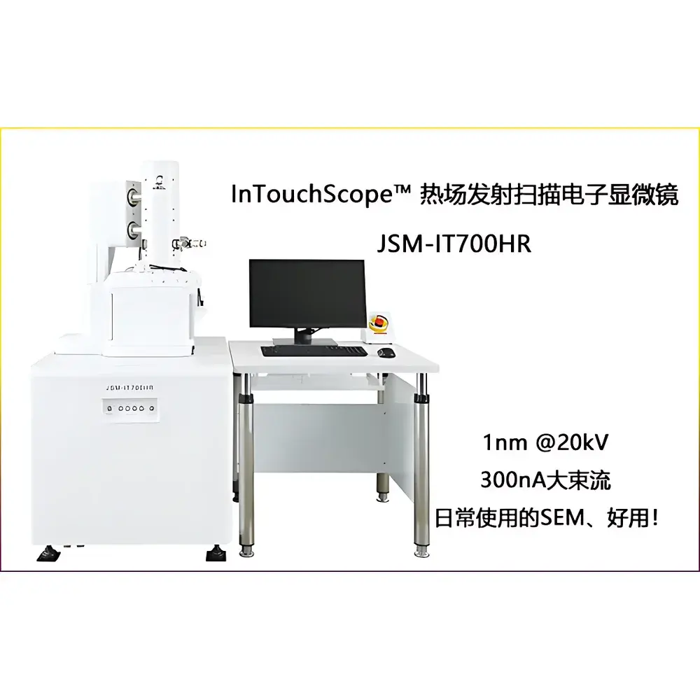
| Brand | JEOL |
|---|---|
| Origin | Japan |
| Model | JSM-IT710HR |
| Instrument Type | Benchtop SEM |
| Electron Source | Thermal Field Emission Gun (TFEG) |
| Secondary Electron Resolution | 1 nm @ 30 kV |
| Backscattered Electron Resolution | 2 nm @ 30 kV |
| Accelerating Voltage | 0.1–30 kV |
| Maximum Magnification | 1,000,000× |
| Probe Current | Up to 300 nA |
| Sample Chamber | Large-volume, front-loading with wide-access door |
| Operating Modes | High Vacuum / Low Vacuum (LV/LA variants available) |
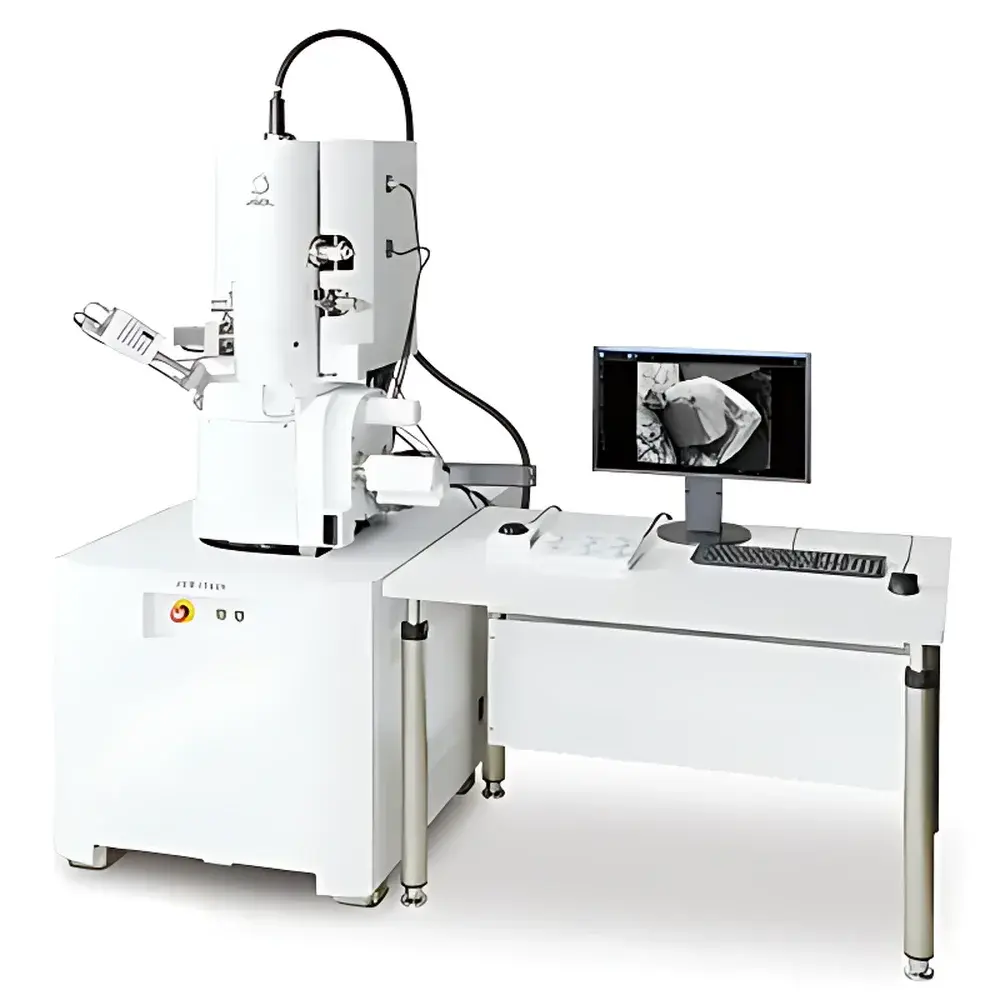
| Brand | JEOL |
|---|---|
| Origin | Japan |
| Model | JSM-IT800 |
| Instrument Type | Floor-Standing SEM |
| Electron Source | Thermal Field-Emission Gun (TFEG) |
| Secondary Electron Resolution | 0.6 nm @ 15 kV, 0.7 nm @ 1 kV |
| Backscattered Electron Resolution | 1.5 nm |
| Accelerating Voltage Range | 0.01–30 kV |
| Maximum Magnification | 2,000,000× (real) |
| Specimen Diameter Capacity | 150 mm |
| Stage Type | 5-Axis Motorized Precision Stage |
| Detector Configuration | In-lens SE detector, upper-stage BSE detector, optional EDS/WDS integration |
| Beam Current | ≥300 nA @ 15 kV |
| Objective Lens Design | Super Hybrid Objective Lens (Magnetic-Field-Free) |
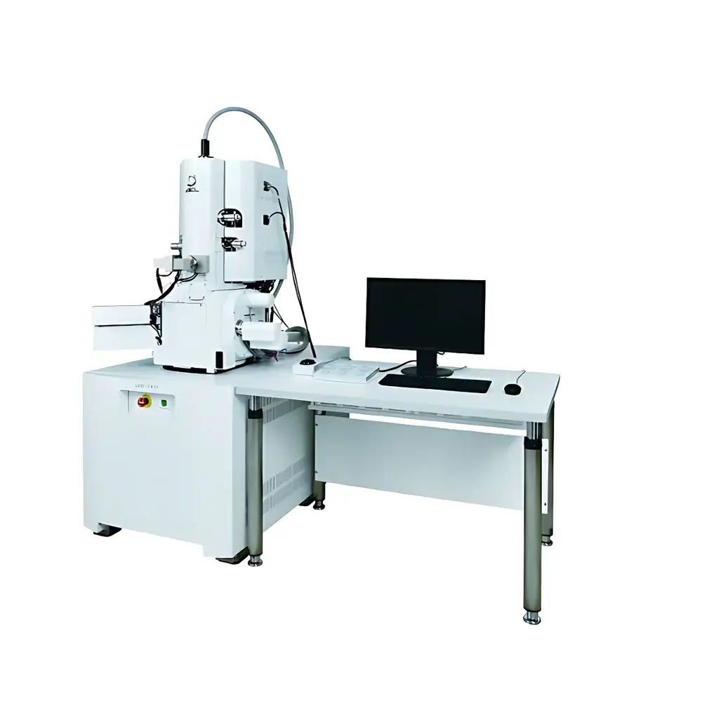
| Brand | JEOL |
|---|---|
| Origin | Japan |
| Model | JSM-IT810 |
| Instrument Type | Floor-standing SEM |
| Electron Gun | Thermal Field Emission (TFE) |
| Secondary Electron (SE) Resolution | 0.5 nm at 15 kV |
| Backscattered Electron (BSE) Resolution | 1.5 nm at 15 kV |
| Accelerating Voltage Range | 0.01–30 kV |
| Magnification Range | ×27 to ×5,480,000 (at 1280 × 960 pixels) |
| Beam Current | Up to 500 nA |
| Detector Configuration | Standard In-lens SE, Through-the-lens BSE, and Optional EDS/EBSD Integration |
| Sample Chamber | Expandable with Multiple Ports for In-situ & Analytical Add-ons |
| Stage | Motorized, High-Precision 5-Axis Tilt/Rotation/Translation Stage |
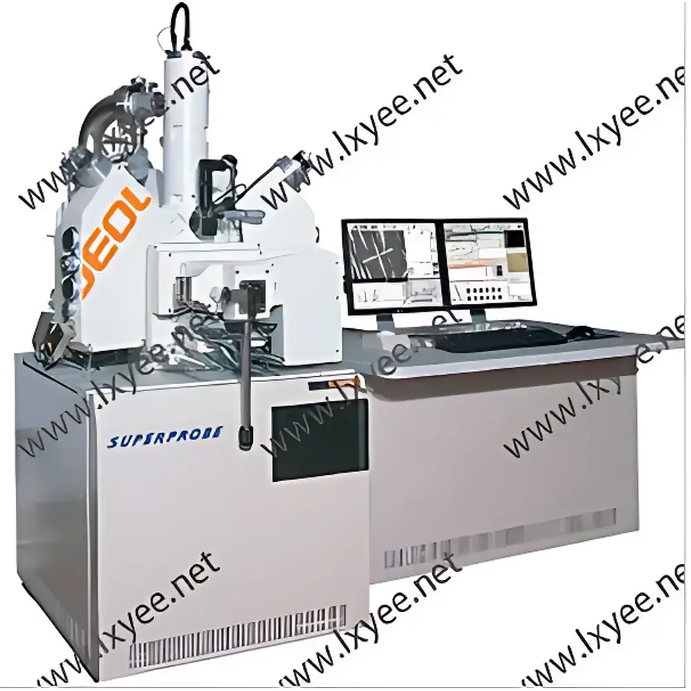
| Brand | JEOL (Japan Electron Optics Laboratory) |
|---|---|
| Origin | Japan |
| Model | JXA-iHP100 |
| Acceleration Voltage | 0–30 kV (0.1 kV step) |
| Beam Current Range | 10⁻¹² – 10⁻⁵ A |
| Beam Current Stability | ±5% / h, ±0.3% / 12 h (W) |
| Secondary Electron Resolution | 6 nm (W), 5 nm (LaB₆) at WD = 11 mm, 30 kV |
| Scan Magnification | ×40 – ×300,000 (WD = 11 mm) |
| Max. Image Resolution | 5,120 × 3,840 pixels |
| Display | Dual LCDs (1,280 × 1,024 each) for EPMA and SEM/EDS operation |
| Optical Microscope Resolution | ~1 µm |
| Depth of Field | ~1 µm |
| Vacuum System | Mechanical pump + turbomolecular pump + ion pump |
| Chamber Vacuum | <8.0 × 10⁻⁴ Pa |
| Gun Vacuum | <9.0 × 10⁻⁵ Pa |
| Elemental Detection Range | WDS: Be (optional) to U |
| EDS | B to U |
| WDS Wavelength Range | 0.087–9.3 nm |
| EDS Energy Range | 0–20 keV |
| WDS Spectrometer Channels | 1–5 (configurable) |
| EDS Detector | One SDD (Silicon Drift Detector), fanless option available |
| Max. Sample Size | 100 mm × 100 mm × 50 mm (H) |
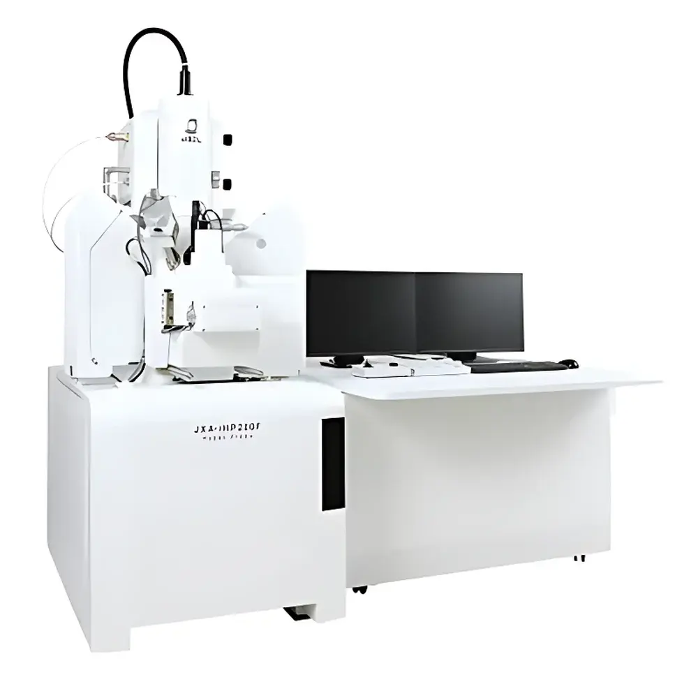
| Brand | JEOL |
|---|---|
| Origin | Japan |
| Model | JXA-iHP200F |
| Instrument Type | Floor-standing, High-Performance EPMA |
| Electron Source | Thermal Field-Emission Gun (TFEG) |
| Secondary Electron Resolution | 2.5 nm at 15 kV |
| Magnification Range | 40× to 300,000× |
| Accelerating Voltage | 1–30 kV |
| Backscattered Electron Imaging | High-Contrast Mode |
| Maximum Sample Dimensions | 100 mm × 100 mm × 50 mm (H) |
| Motorized Stage | 5-Axis Precision Drive |
| Standard Detectors | Solid-State Backscatter Detector, Wavelength-Dispersive Spectrometer (WDS), Energy-Dispersive Spectrometer (EDS) |
| Vacuum System | Ultra-High Vacuum (UHV) Compatible |
| Interface Expansion | Multiple Dedicated Ports for Optional Analyzers (e.g., EBSD, CL, STEM-in-SEM) |
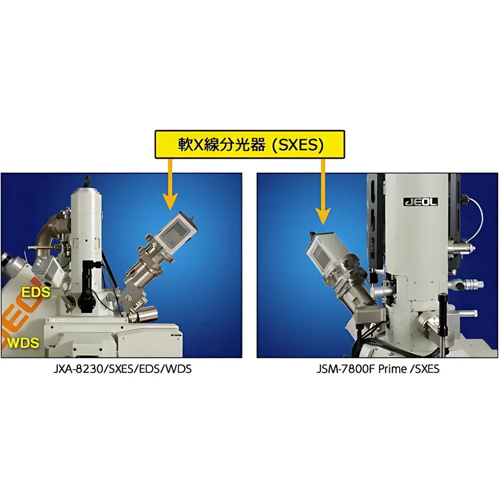
| Brand | JEOL |
|---|---|
| Origin | Japan |
| Manufacturer Type | Authorized Distributor |
| Origin Category | Imported |
| Model | SXES |
| Price | USD 700,000 |
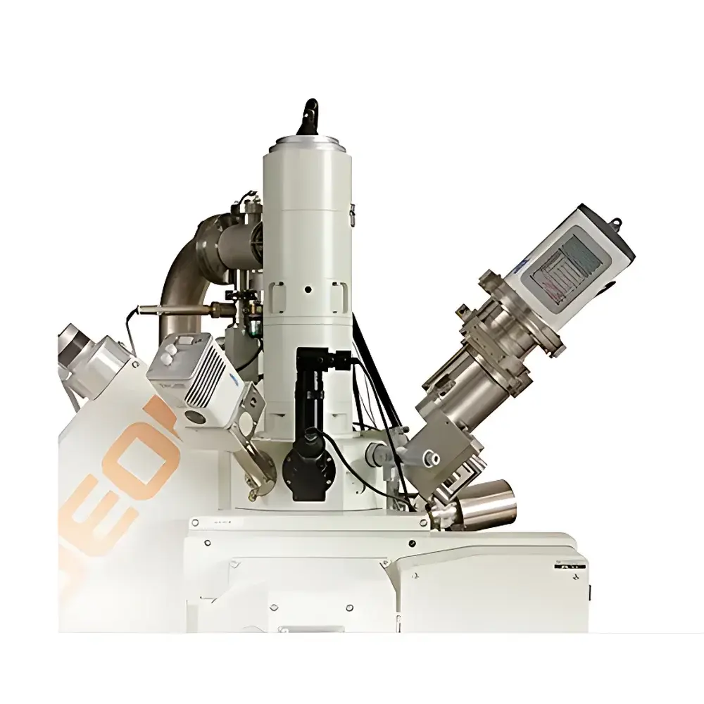
| Brand | JEOL |
|---|---|
| Origin | Japan |
| Model | SXES |
| Energy Resolution | 0.3 eV (at Al-L edge, 73 eV) |
| Detection Energy Range | 50–170 eV (JS50XL grating) / 70–210 eV (JS50XL grating) |
| Mounting Interface | EPMA WDS Port #2 (front right) or FE-SEM WDS port (front left-rear) |
| Dimensions (W×D×H) | 168 mm × 348 mm × 683 mm (including CCD distance from interface) |
| Weight | 25 kg |
| Compatible Instruments | EPMA — JXA-8530F, JXA-8230, JXA-8500F, JXA-8200 |
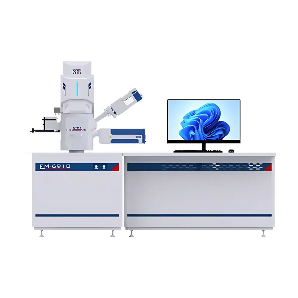
| Brand | KYKY |
|---|---|
| Origin | Beijing, China |
| Manufacturer Type | Direct Manufacturer |
| Instrument Class | Floor-Standing Conventional SEM |
| Electron Source | Tungsten Filament |
| SEM Category | Entry-Level Tungsten-Filament SEM |
| Secondary Electron (SE) Resolution | 3 nm @ 30 kV, 8 nm @ 3 kV |
| Accelerating Voltage Range | 0.2–30 kV |
| Backscattered Electron (BSE) Resolution | 4 nm @ 30 kV |
| Sample Chamber | Optional Large-Capacity Chamber |
| Vacuum Mode | Compatible with Low-Vacuum Module |
| Load Lock System | Max. Sample Diameter ≤75 mm, Height ≤15 mm |
| Navigation Camera | Integrated Wide-Field CCD Navigation Camera |
| Imaging Modes | Simultaneous SE/BSE Dual-Channel Imaging |
| Image Stitching | Automated Full-Field Matrix Acquisition & Real-Time High-Throughput Mosaic Reconstruction |
| Particle Analysis | AI-Driven Morphometric Quantification (size, aspect ratio, circularity, convexity, Feret diameter, etc.) with Auto-Scale Calibration |
| Metrology Tools | Distance, Angle, Line (horizontal/vertical), Circle Diameter, and Profile Analysis |
| Electron Beam Lithography (EBL) Capability | Integrated Vector-Scan EBL Subsystem Supporting Pattern Definition, Dose Control, and Concurrent SEM Observation |
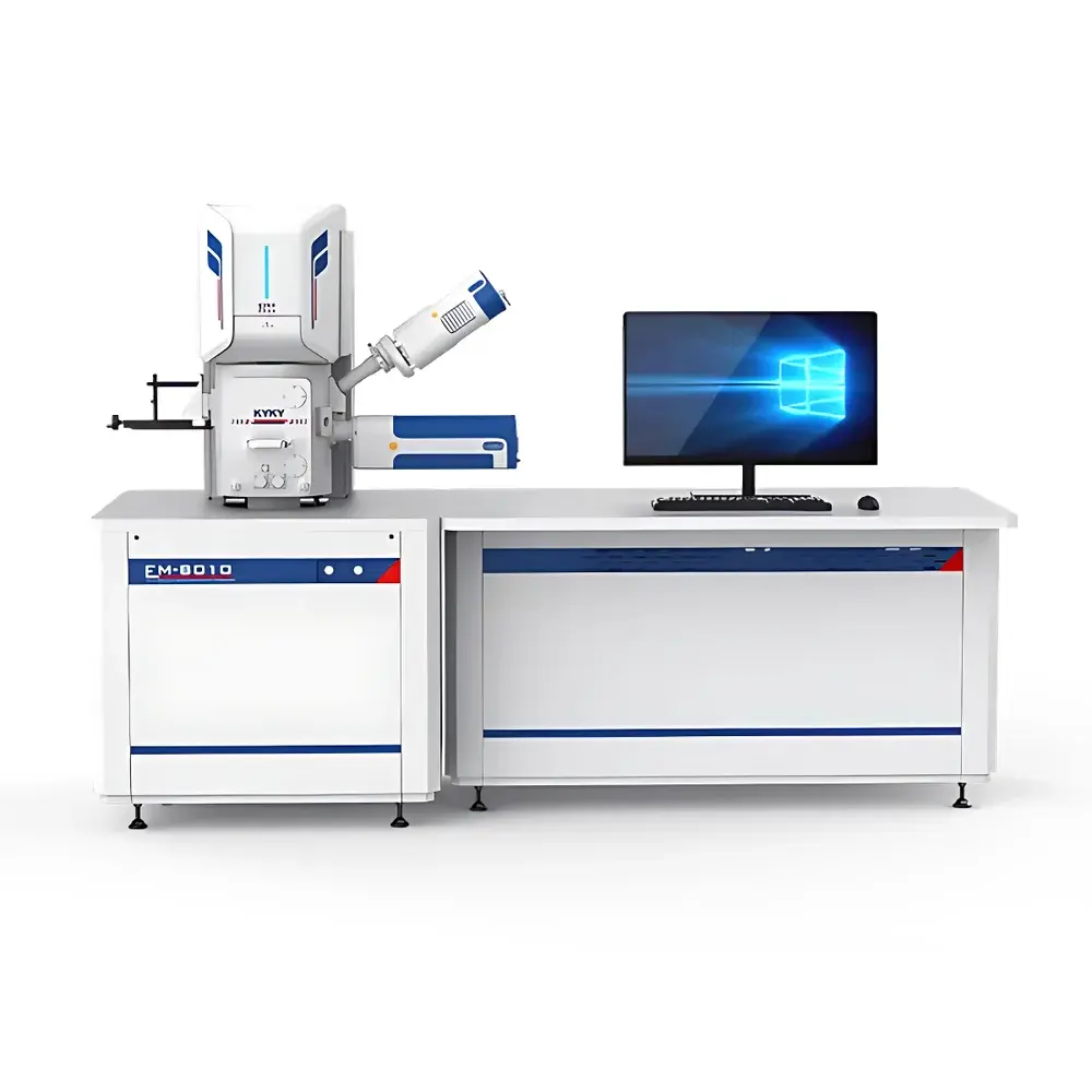
| Brand | KYKY |
|---|---|
| Origin | Beijing, China |
| Manufacturer Type | Direct Manufacturer |
| Instrument Type | Floor-standing SEM |
| Electron Gun Type | Schottky Thermal Field Emission |
| SEM Class | Entry-level Field Emission SEM |
| Secondary Electron Resolution | 1.5 nm @ 15 kV |
| Accelerating Voltage Range | 0.2–30 kV |
| Backscattered Electron Resolution | 3 nm @ 30 kV |
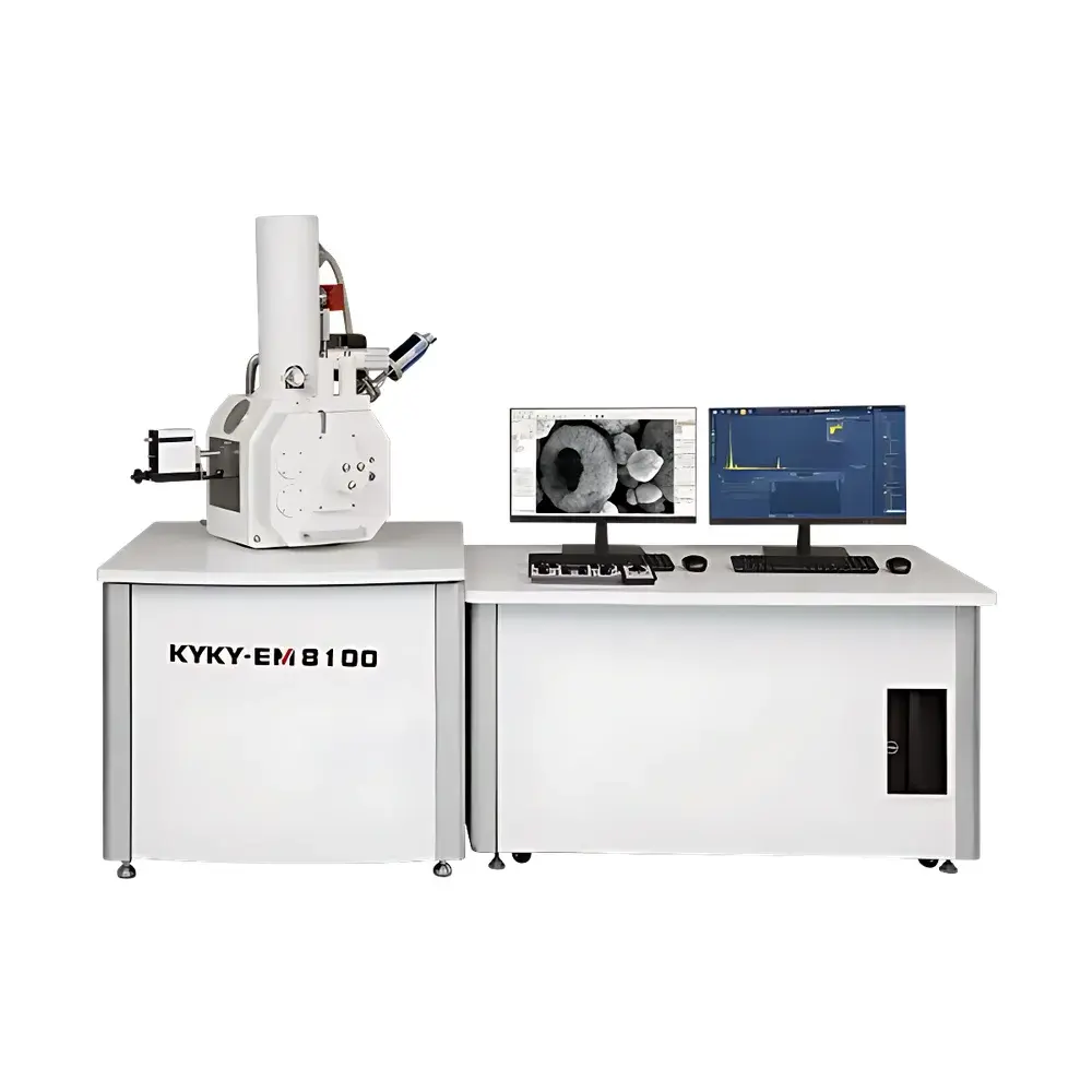
| Brand | KYKY |
|---|---|
| Origin | Beijing, China |
| Manufacturer Type | Original Equipment Manufacturer (OEM) |
| Instrument Type | Floor-Model SEM |
| Electron Gun | Thermal Field-Emission (TFE) |
| SEM Class | High-Resolution Field-Emission SEM |
| Secondary Electron (SE) Resolution | 0.9 nm @ 30 kV |
| Magnification Range | 1×–3,000,000× (optical: 1×–100×) |
| Accelerating Voltage | 0.2–30 kV |
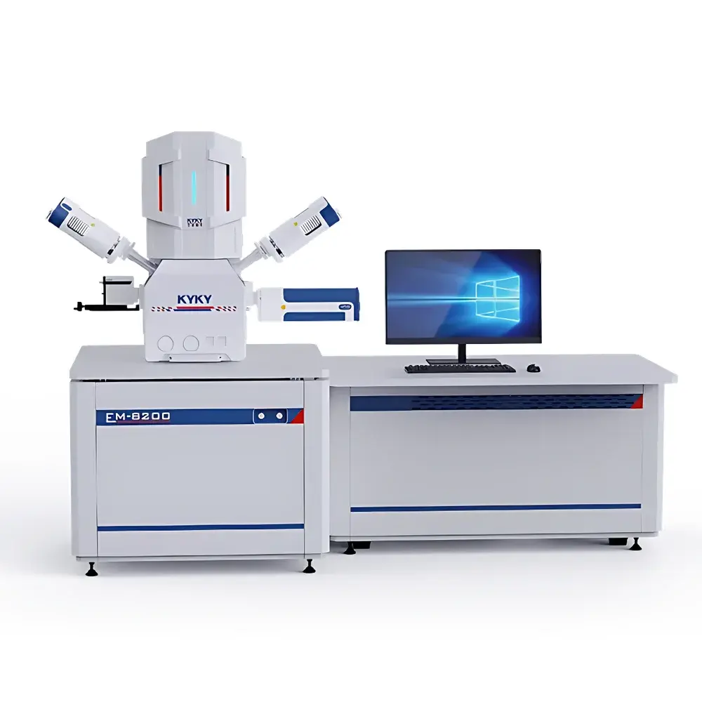
| Brand | KYKY |
|---|---|
| Origin | Beijing, China |
| Manufacturer Type | Direct Manufacturer |
| Instrument Type | Floor-Standing SEM |
| Electron Gun | Thermal Field Emission |
| SEM Class | Ultra-High-Resolution Field Emission |
| Secondary Electron Resolution | 0.8 nm @ 15 kV, 1.5 nm @ 1 kV |
| Magnification Range | 1×–3,000,000× (electronic), 1×–100× (optical) |
| Accelerating Voltage | 0.2–30 kV |
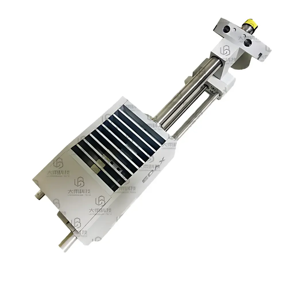
| Brand | LARGEBEAM |
|---|---|
| Origin | USA |
| Manufacturer Type | OEM Manufacturer |
| Import Status | Imported |
| Model | RIIDEye |
| Pricing | Upon Request |
| Detector Type | 2×2 NaI(Tl) scintillator & 1.5×1.5″ LaBr₃(Ce) crystal |
| Energy Range | 20 keV – 3 MeV |
| Display | 3.5″ TFT-LCD, 320×240 resolution, 32,000-color backlight |
| Battery Life | 8 hours (rechargeable Li-ion), with 6 spare AA battery slots |
| Weight | 2.6 kg (5.7 lb) with NaI configuration |
| Dimensions | 27.9 × 12.0 × 21.9 cm (11.0 × 4.7 × 8.6 in) |
| Operating Temperature | −20 °C to +50 °C (−4 °F to 122 °F) |
| Neutron Detection | 1.8 × 3.4 cm Ce-doped Cs₂LiYCl₆ (CLYC) crystal |
| Isotope Library | 47 nuclides |
| Trigger Modes | ANSI, ANSI+, Security, Medical, Industrial, User-Defined |
| Stabilization | Automatic K-40 background compensation, no external reference source required |
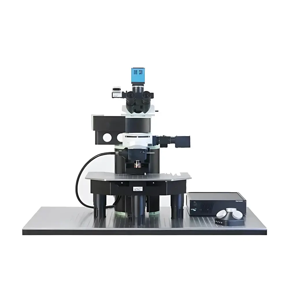
| Brand | LaVision GmbH |
|---|---|
| Country of Origin | Germany |
| Model | TriM Scope |
| Scan Mode Flexibility | Single-beam to multi-beam configurable scanning |
| Software Control | ImSpector Pro with millisecond-scale region switching |
| Detection Channels | Up to 8 non-descanned detectors (NDDs) |
| Detector Options | Cooled Generation III GaAsP PMTs or APDs |
| Quantum Efficiency Gain | Up to 40% higher than standard PMTs |
| OPO Compatibility | Full integration support for optical parametric oscillator excitation sources |
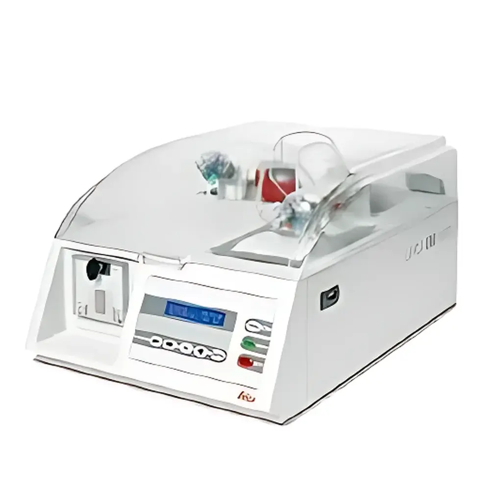
| Brand | Leica |
|---|---|
| Origin | Austria |
| Model | EM AC20 |
| Capacity | 20 grids per cycle |
| Reagent Consumption | ~6 mL per cycle (uranyl acetate + lead citrate) |
| Predefined Programs | 10 staining + 2 cleaning protocols |
| Temperature Control Range | 20–60 °C |
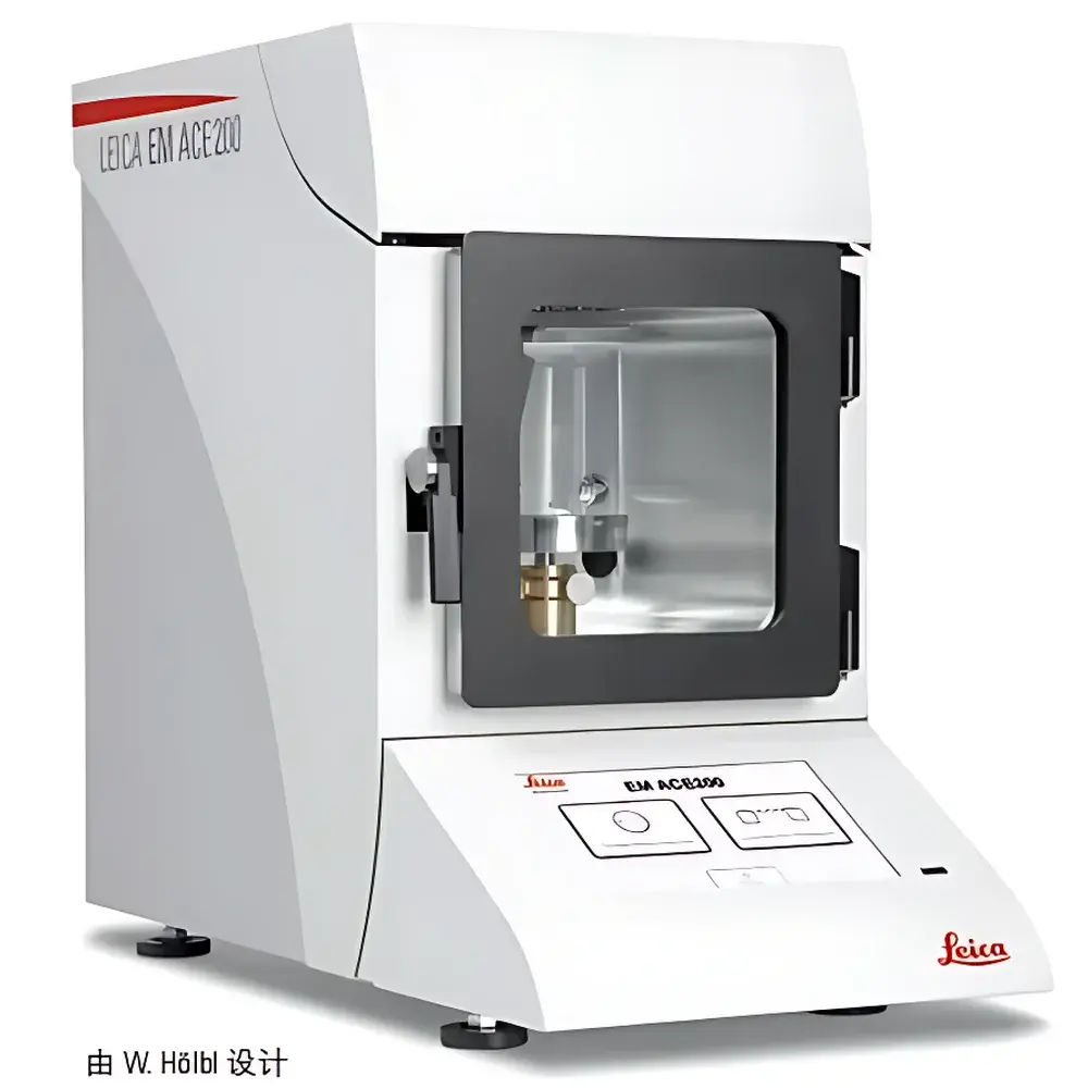
| Brand | Leica |
|---|---|
| Origin | Germany |
| Model | EM ACE200 |
| Configuration Options | Sputter Coating / Carbon Evaporation / Dual-Source Interchangeable Setup |
| Optional Modules | Quartz Crystal Thickness Monitor, Planetary Rotating Stage, Glow Discharge Unit |
| Brand | Leica |
|---|---|
| Origin | Austria |
| Model | EM ACE200 |
| Vacuum Level | 7 × 10⁻³ mbar |
| Sputtering Current Range | 0–150 mA |
| Sample Chamber Dimensions | 140 mm (W) × 145 mm (D) × 150 mm (H) |
| Working Distance Adjustment | 30–100 mm |
| Carbon Evaporation Mode | Pulsed, Precise Thickness Control |
| Optional Quartz Crystal Thickness Monitor | ±0.1 nm resolution |
| Optional Glow Discharge Function | For hydrophilization of TEM grids |
| Control Interface | Full-touch LCD panel with automated vacuum/pumping/coating/venting sequence |
| Brand | Leica |
|---|---|
| Origin | Germany |
| Model | EM ACE200 |
| Vacuum Level | 7×10⁻³ mbar |
| Sputtering Current Range | 0–150 mA |
| Sample Chamber Dimensions | 140 mm (W) × 145 mm (D) × 150 mm (H) |
| Working Distance Adjustment | 30–100 mm |
| Carbon Evaporation Mode | Pulsed, Quartz Crystal Thickness Monitor Optional (±0.1 nm resolution) |
| Operation Interface | Touchscreen with Fully Automated Cycle Control (Pump-down → Coating → Venting) |
| Dual-Mode Capability | Sputtering + Carbon Evaporation |
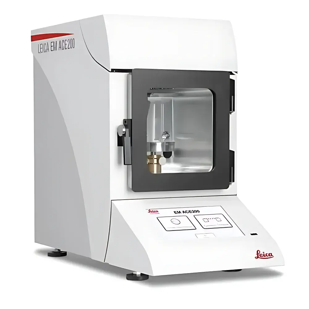
| Brand | Leica |
|---|---|
| Origin | Germany |
| Model | EM ACE200 |
| Vacuum Level | ≤7 × 10⁻³ mbar |
| Chamber Dimensions (W×D×H) | 140 mm × 145 mm × 150 mm |
| Sample Stage Diameter | 80 mm |
| Working Distance | 30–100 mm |
| Sputtering Current | ≤150 mA |
| Film Thickness Resolution (with QCM option) | 0.1 nm |
| Coating Modes | Ion Sputtering, Carbon Wire Evaporation, Dual-Mode, Optional Glow Discharge |
| Optional Features | Quartz Crystal Microbalance (QCM), Planetary Rotation, Interchangeable Shields, Directional Sputtering, Pulsed Carbon Evaporation |
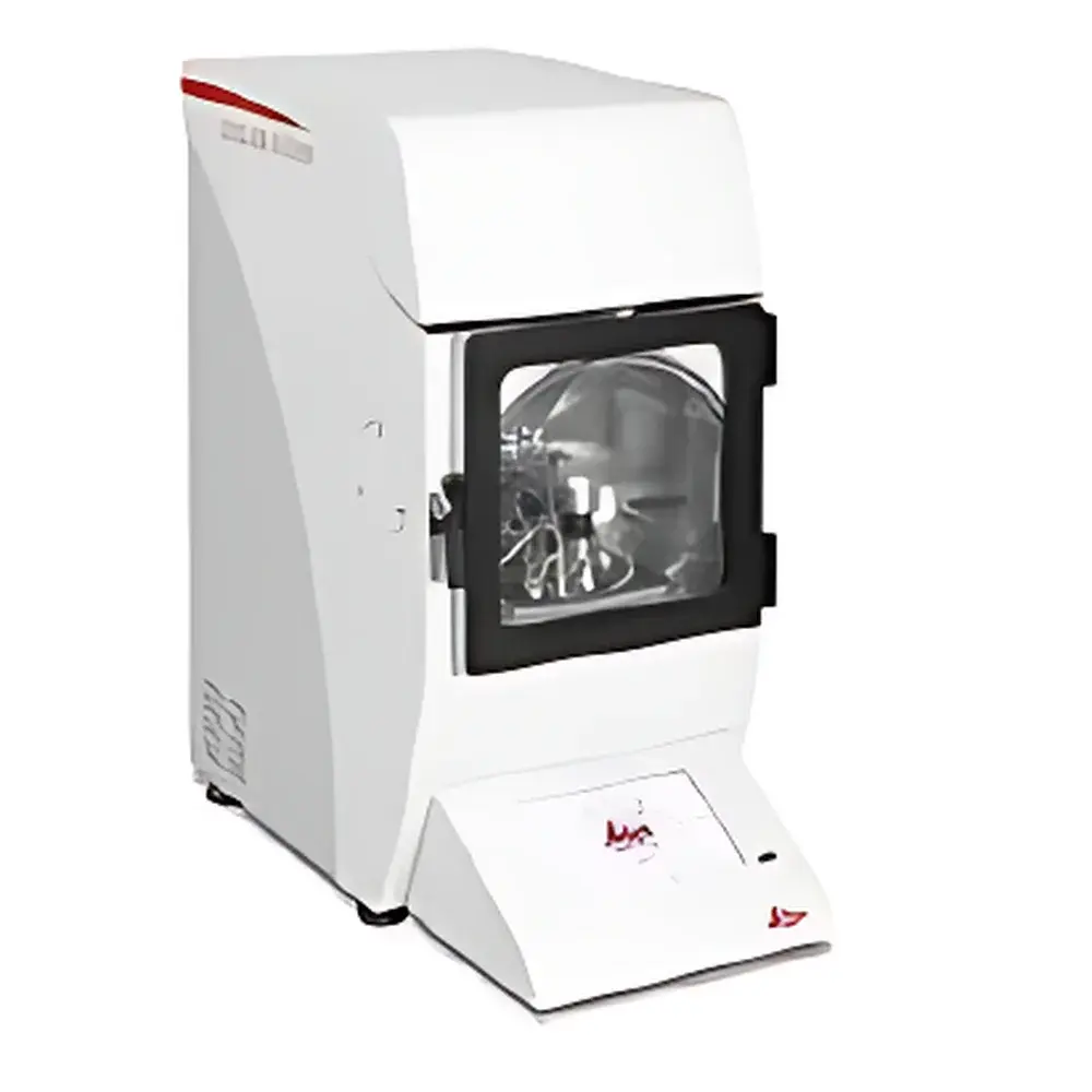
| Brand | Leica |
|---|---|
| Origin | Austria |
| Model | EM ACE600 |
| Vacuum Level | 2 × 10⁻⁶ mbar |
| Pumping System | Diaphragm Pump + Turbo Molecular Pump (Oil-Free) |
| Thickness Control | Quartz Crystal Monitor (Resolution: 0.1 nm) |
| Sputtering Current Range | 0–150 mA |
| Chamber Dimensions | 200 mm (W) × 150 mm (D) × 195 mm (H) |
| Sample Stage | Motorized Rotation + Adjustable Working Distance (30–100 mm) |
| Coating Modes | Ion Sputtering, Carbon Filament Evaporation, Carbon Rod (Resistive) Evaporation, Electron Beam Evaporation, Dual-Source Configurations (e.g., Sputter + E-beam), Glow Discharge (Optional) |
| Compatibility | EM VCT100 Cryo-Transfer System |
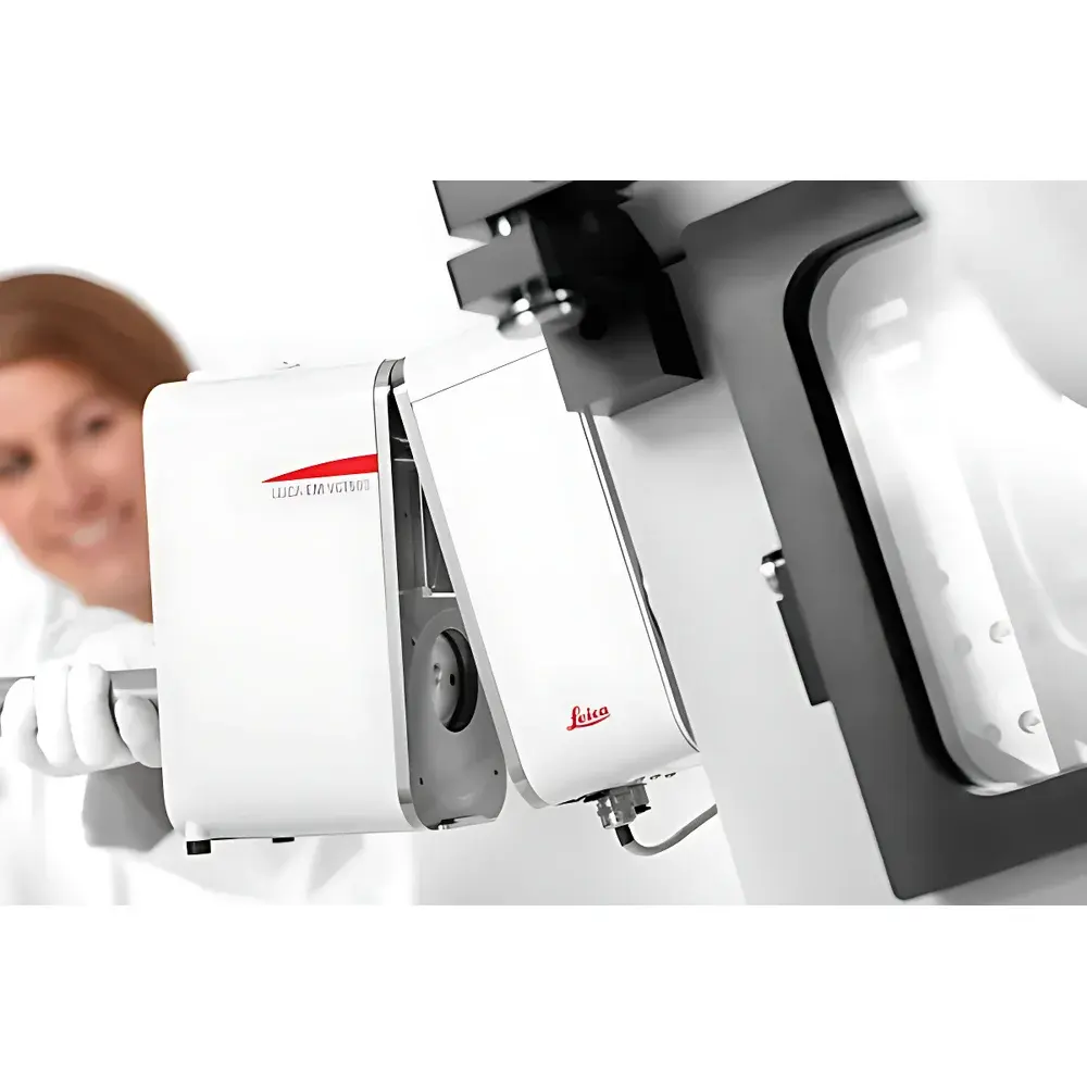
| Brand | Leica |
|---|---|
| Origin | Austria |
| Model | EM ACE900 |
| Application | Cryo-SEM & TEM Sample Preparation |
| Cooling Medium | Liquid Nitrogen (LN₂) |
| Vacuum System | Dual-chamber with Load-Lock Transfer |
| Coating | Electron Beam Evaporation for Carbon/Metal Replicas |
| Compatibility | Integrated with Leica EM VCT500 Cryo-Transfer System |
| Environmental Certification | DIN EN ISO 14001 |
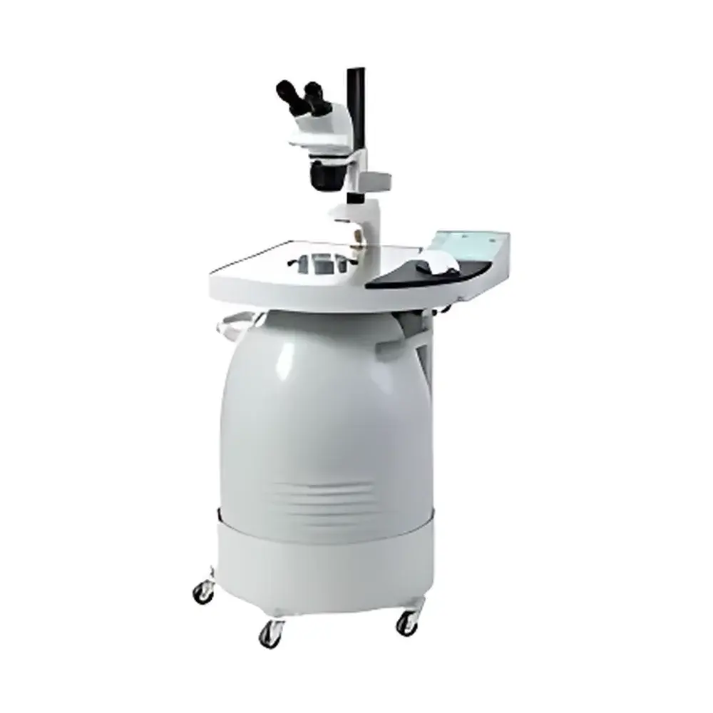
| Brand | Leica |
|---|---|
| Origin | Austria |
| Model | EM AFS2 |
| Temperature Range | –140 °C to +70 °C (precisely controlled) |
| Liquid Nitrogen Capacity | 35 L (supports up to 5 days of continuous operation) |
| Deep Freeze Mode | < –140 °C for cryo-transfer |
| TF (Trace-free) Mode | Active O₂/H₂O removal |
| UV Polymerization | Integrated LED UV source (365 nm) |
| User Storage | 10 user profiles, 99 programs per user |
| Interface | Full-color graphical touchscreen with mouse control |
| Safety | Built-in exhaust system for hazardous solvent vapors |
| Optional Module | Leica EM FSP Fluid Service Processor (automated reagent dispensing, dilution, exchange, and UV polymerization) |
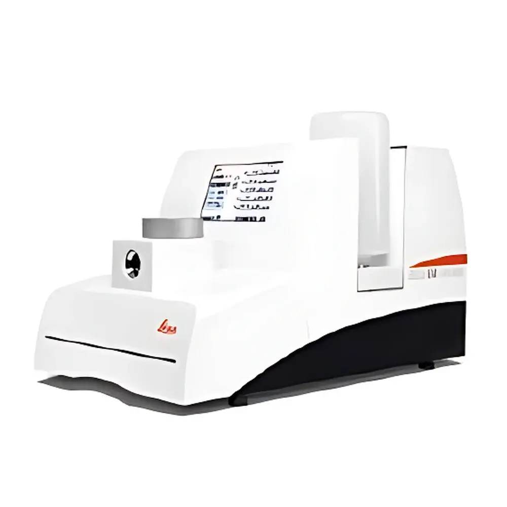
| Brand | Leica |
|---|---|
| Origin | Austria |
| Model | EM CPD300 |
| Sample Chamber Volume | 175 mL |
| Control Interface | Touchscreen |
| CO₂ Consumption | Reduced via proprietary filler material |
| Safety Features | Integrated waste liquid separation, software-controlled venting interlock |
| Automation Level | Fully automated critical point drying cycle |
| Compliance | Designed for GLP-compliant SEM sample preparation workflows |
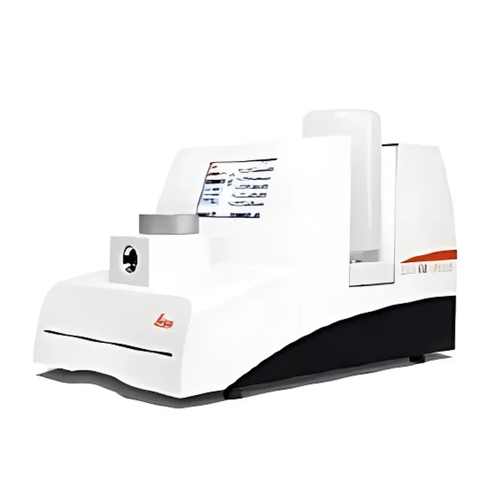
| Brand | Leica |
|---|---|
| Origin | Austria |
| Model | EM CPD300 |
| Sample Chamber Volume | 175 mL |
| Control Interface | Touchscreen with Embedded Process Logic |
| CO₂ Efficiency | Optimized via Patented Fill Medium Design |
| Safety Systems | Dual-Pressure Interlocks, Integrated Waste Fluid Separation, Automatic Venting Safeguards |
| Compliance | Designed to Support GLP/GMP Workflow Integrity and ISO 13485-Aligned Lab Documentation Requirements |
| Pricing Range | USD 65,000 – 105,000 (FOB Austria) |