
Electron Microscope
Filter
Showing 151–180 of 532 results
| Brand | Hitachi |
|---|---|
| Origin | Japan |
| Manufacturer | Hitachi High-Tech Corporation |
| Type | Atomic Force Microscope (AFM) |
| Model | AFM100 |
| Instrument Category | Materials-Grade AFM |
| Position Detection Noise | 0.03 nm |
| Maximum Sample Diameter | ≤35 mm |
| Maximum Sample Thickness | ≤10 mm |
| Sample Stage Travel Range | 5 mm |
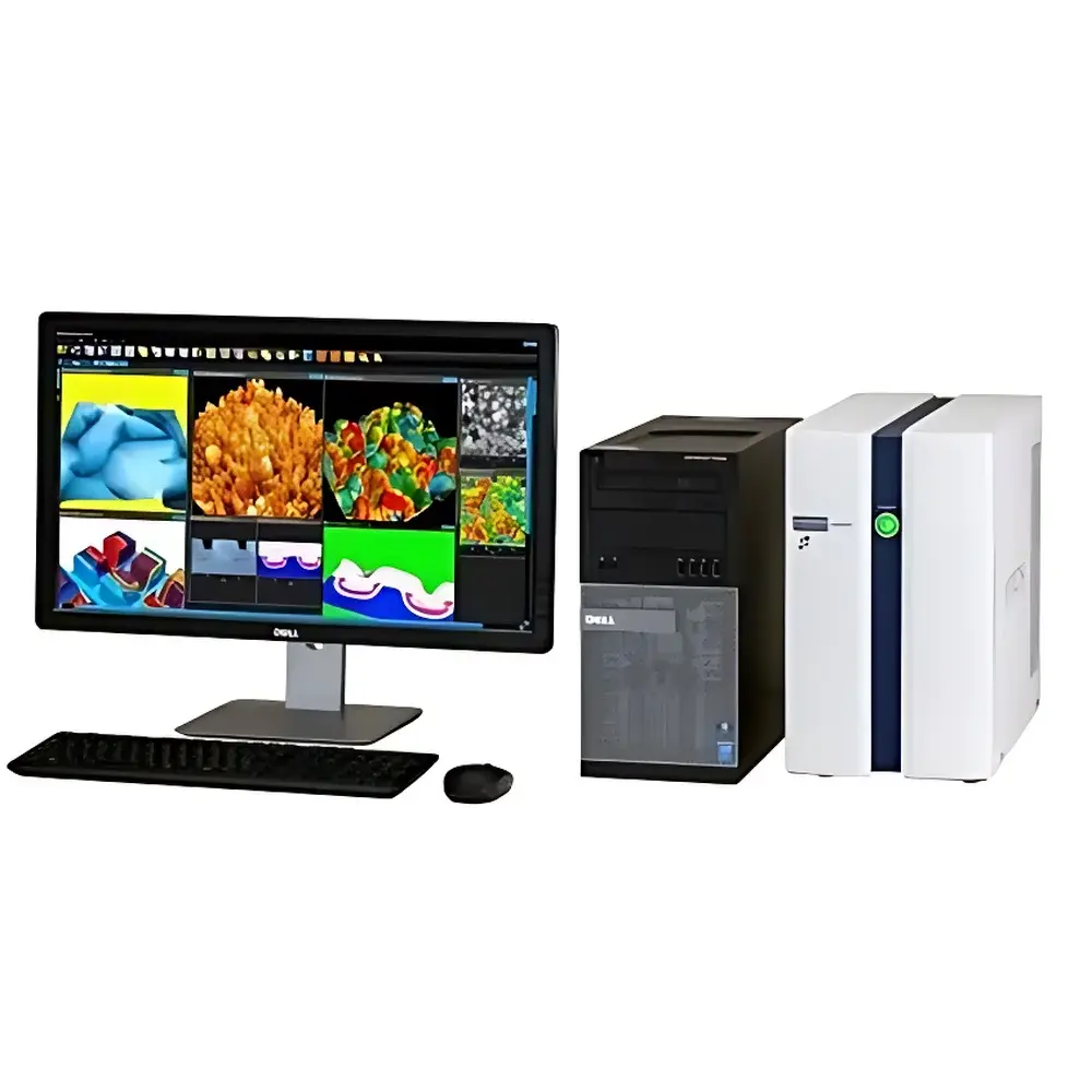
| Brand | Hitachi |
|---|---|
| Origin | Japan |
| Manufacturer | Hitachi High-Tech Science Corporation |
| Product Type | Atomic Force Microscope (AFM) Controller |
| Model | AFM5000II / RealTune®II |
| Compliance | Designed for ISO/IEC 17025-compliant labs |
| Software Architecture | Windows-based real-time control platform with audit trail capability |
| Control Resolution | Sub-nanometer positioning accuracy |
| Vibration Noise Floor | < 0.1 nm RMS (in closed-loop mode) |
| Sample Stage Travel Range | X/Y: ±25 µm, Z: ±5 µm |
| GUI Framework | Qt-based modular interface with tabbed workflow navigation |
| 3D Rendering Engine | OpenGL-accelerated volumetric reconstruction |
| Data Format | HDF5-compliant binary + metadata-rich XML header |
| Regulatory Alignment | Supports FDA 21 CFR Part 11 electronic signature and ALCOA+ data integrity principles |
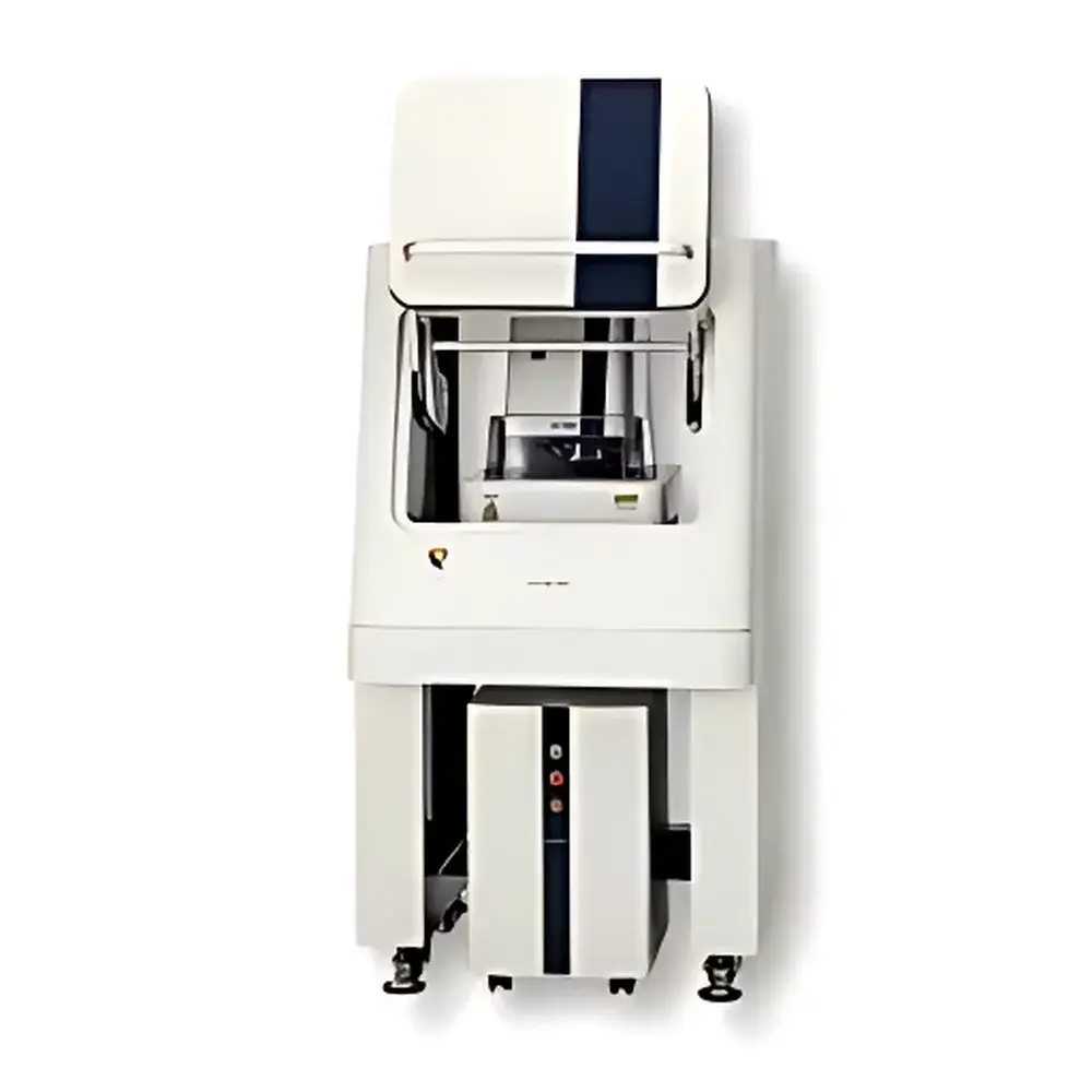
| Brand | Hitachi |
|---|---|
| Origin | Japan |
| Manufacturer Type | Original Equipment Manufacturer (OEM) |
| Product Category | Imported Instrument |
| Model | AFM5500M II |
| Instrument Type | Atomic Force Microscope (AFM) |
| Application Class | Materials Science AFM |
| Position Detection Noise | ≤ 0.04 nm (High-Resolution Mode) |
| Sample Diameter | ≤ 100 mm |
| Sample Thickness | ≤ 20 mm |
| XY Stage Travel Range | 100 mm × 100 mm |
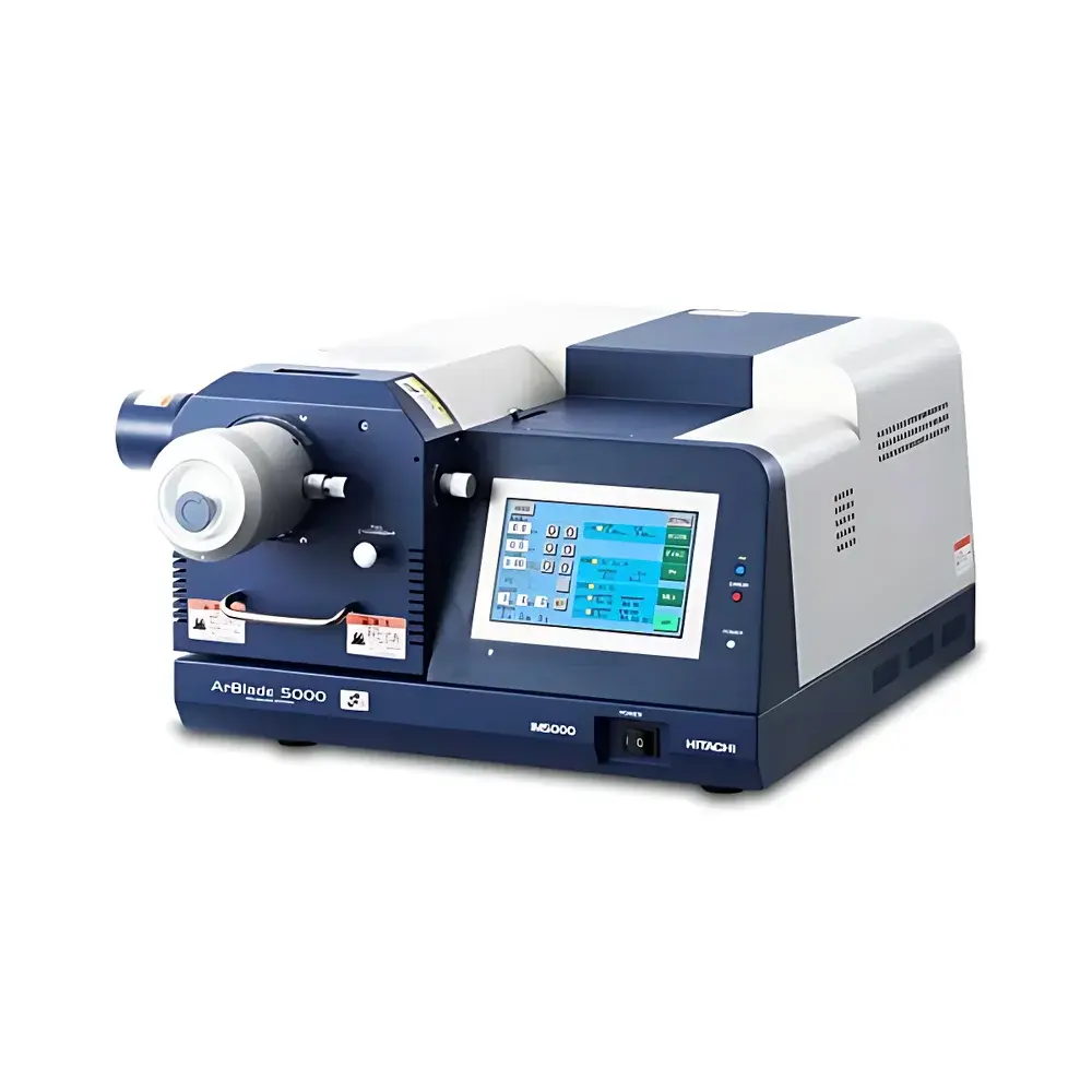
| Brand | Hitachi |
|---|---|
| Origin | Japan |
| Manufacturer | Hitachi High-Tech Corporation |
| Type | Imported Equipment |
| Model | ArBlade5000 |
| Price Range | USD 135,000 – 270,000 (FOB Japan) |
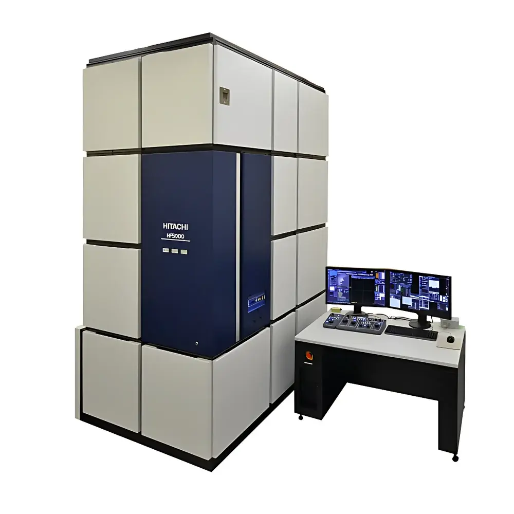
| Brand | Hitachi |
|---|---|
| Origin | Japan |
| Manufacturer Type | Original Equipment Manufacturer (OEM) |
| Product Origin | Imported |
| Model | HF5000 |
| Accelerating Voltage | Up to 200 kV |
| Magnification | TEM (×200–×4,000,000), STEM (×20–×4,000,000) |
| HAADF-STEM Resolution | 0.78 Å |
| EDS Solid Angle | Up to 2.0 sr (dual-windowless silicon drift detectors) |
| Imaging Modes | TEM, STEM, SEM, Selected-Area Electron Diffraction (SAED), Convergent-Beam Electron Diffraction (CBED) |
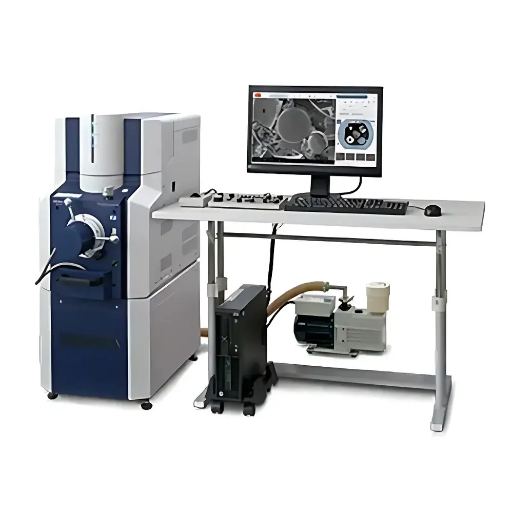
| Brand | Hitachi High-Tech |
|---|---|
| Origin | Japan |
| Manufacturer | Hitachi High-Technologies Corporation |
| Product Type | Imported Desktop SEM |
| Model | FlexSEM 1000 II |
| Electron Source | Tungsten Filament |
| Secondary Electron Resolution | 4.0 nm @ 20 kV (High Vacuum), 15.0 nm @ 1 kV (High Vacuum) |
| Backscattered Electron Resolution | 5.0 nm @ 20 kV (Low Vacuum) |
| Magnification Range | 6×–300,000× (Film Equivalent), 16×–800,000× (Display) |
| Accelerating Voltage | 0.3–20 kV |
| EDS Detector | 30 mm² Silicon Drift Detector (SDD), Nitrogen-free |
| Dimensions (Main Unit) | 450 mm (W) × 640 mm (D) |
| Power Interface | Standard IEC C13 Socket |
| System Architecture | Modular Main Unit + Detachable Power Supply Unit |
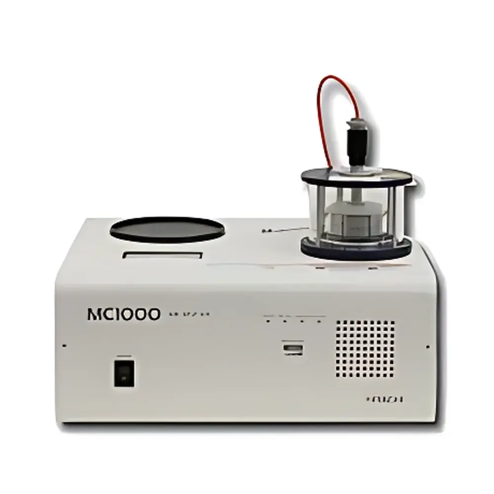
| Brand | Hitachi High-Technologies |
|---|---|
| Origin | Japan |
| Manufacturer | Hitachi High-Technologies Corporation |
| Type | Imported |
| Model | MC1000 |
| Pricing | Upon Request |
| Max Sample Diameter | 60 mm |
| Max Sample Height | 20 mm |
| Control Interface | LCD Touchscreen |
| Memory Function | Yes |
| Optional Accessories | Thick/Large Sample Holder Kit |
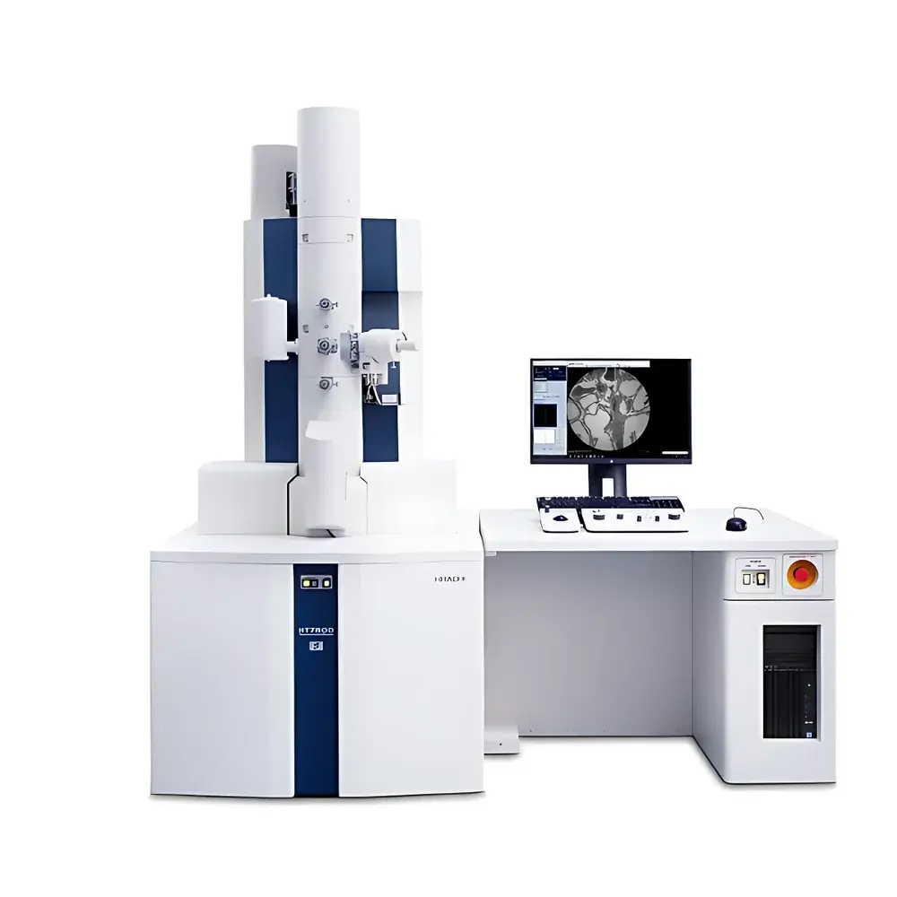
| Brand | Hitachi |
|---|---|
| Origin | Japan |
| Manufacturer Type | Original Equipment Manufacturer (OEM) |
| Product Origin | Imported |
| Model | HT7800 Series |
| Accelerating Voltage | 20–120 kV |
| Magnification Range | ×200–×200,000 (High Contrast Mode) |
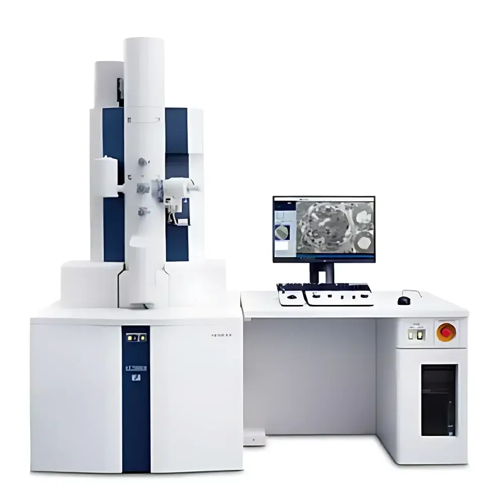
| Brand | Hitachi |
|---|---|
| Origin | Japan |
| Manufacturer | Hitachi High-Tech Corporation |
| Product Type | Imported TEM |
| Model | HT7800II |
| Accelerating Voltage | 20–120 kV |
| Magnification | ×200–×200,000 (High-Contrast Mode) |
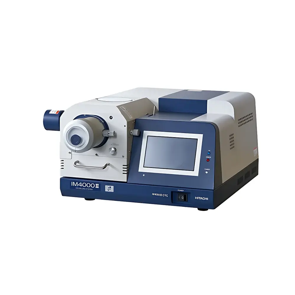
| Brand | Hitachi |
|---|---|
| Origin | Japan |
| Manufacturer | Hitachi High-Tech Corporation |
| Type | Imported Instrument |
| Model | IM4000 II |
| Pricing | Available Upon Request |
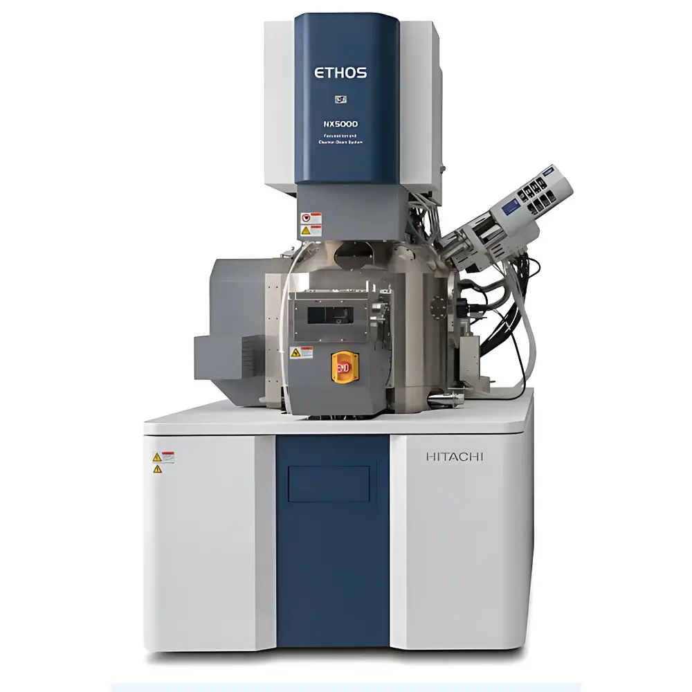
| Brand | Hitachi |
|---|---|
| Origin | Japan |
| Manufacturer | Hitachi High-Tech Corporation |
| Type | Imported Instrument |
| Model | NX5000 |
| Pricing | Available Upon Request |
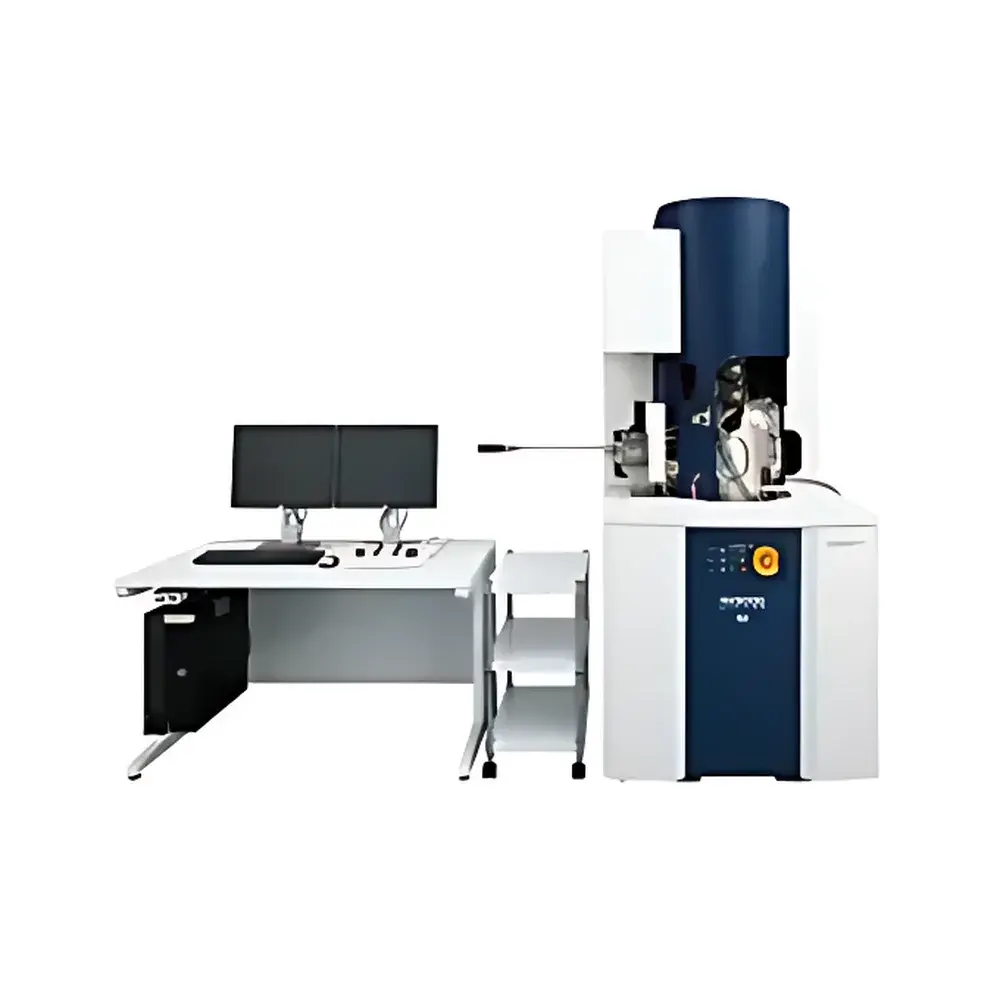
| Brand | Hitachi |
|---|---|
| Origin | Japan |
| Manufacturer | Hitachi High-Tech Corporation |
| Type | Imported Instrument |
| Model | NX9000 |
| Pricing | Available Upon Request |
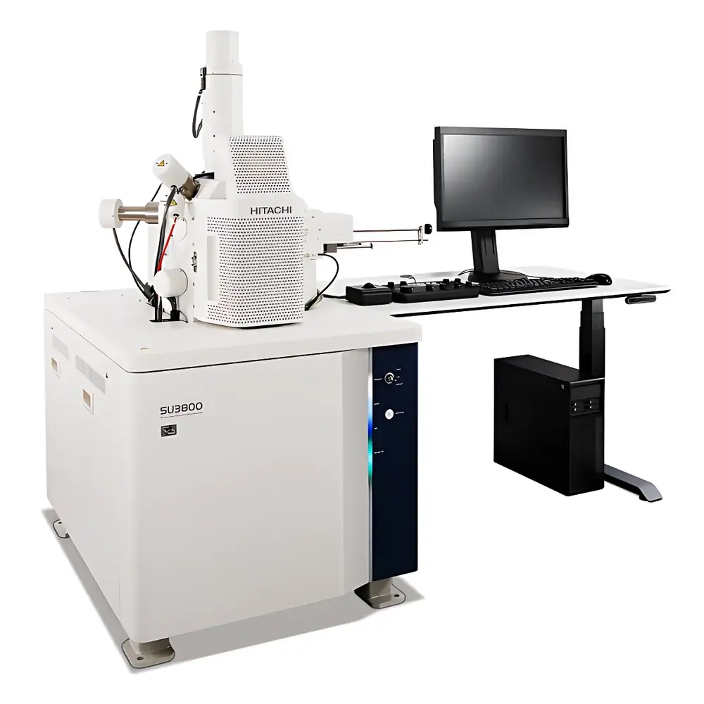
| Brand | Hitachi |
|---|---|
| Origin | Japan |
| Manufacturer Type | Original Equipment Manufacturer (OEM) |
| Import Status | Imported |
| Model | SU3800 |
| Electron Source | Tungsten Filament |
| Secondary Electron Resolution | 3.0 nm at 30 kV |
| Magnification Range | 5–300,000× (low mode), 7–800,000× (high mode) |
| Accelerating Voltage | 0.3–30 kV (standard mode) |
| Backscattered Electron Resolution | 4.0 nm at 30 kV (low-vacuum mode) |
| Maximum Sample Diameter | 200 mm |
| Maximum Sample Height | 80 mm |
| Maximum Sample Weight | 2 kg |
| Navigation System | SEM MAP |
| Automated Imaging | Multi Zigzag Stitching |
| Filament Monitoring | Intelligent Filament Technology (IFT) |
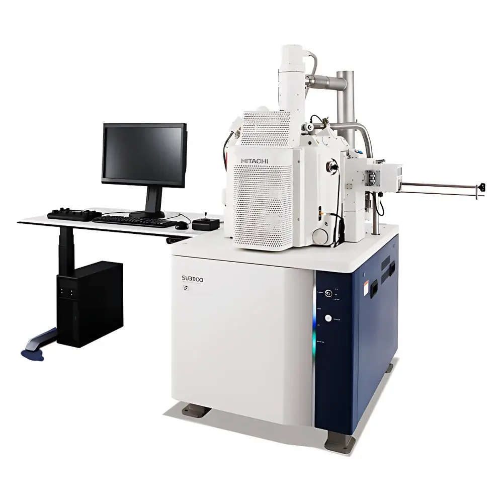
| Brand | Hitachi |
|---|---|
| Origin | Japan |
| Manufacturer | Hitachi High-Tech Corporation |
| Product Type | Imported |
| Model | SU3900 |
| Electron Source | Tungsten Filament |
| Secondary Electron Resolution | 3.0 nm |
| Magnification Range | ×5–300,000 (standard mode), ×7–800,000 (high-magnification mode) |
| Accelerating Voltage | 0.3–30 kV |
| Backscattered Electron Resolution | 4.0 nm @ 30 kV (low-vacuum mode) |
| Maximum Sample Diameter | 300 mm |
| Maximum Sample Height | 130 mm |
| Maximum Sample Weight | 5 kg |
| Navigation Field of View | up to Ø200 mm |
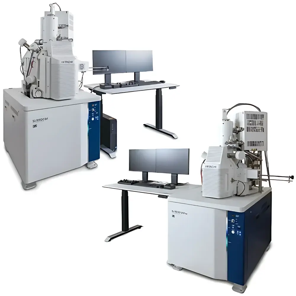
| Brand | Hitachi |
|---|---|
| Origin | Japan |
| Manufacturer Type | Original Equipment Manufacturer (OEM) |
| Product Origin | Imported |
| Model | SU3900/SU3800 SE Series |
| Instrument Type | Floor-Standing Conventional SEM |
| Electron Source | Thermal Field-Emission Gun |
| Secondary Electron Resolution | 0.9 nm @ 30 kV, 2.5 nm @ 1 kV, 1.6 nm @ 1 kV (Deceleration Mode) |
| Magnification Range | ×5 to ×600,000 (Film Equivalent) |
| Accelerating Voltage | 0.5 kV to 30 kV |
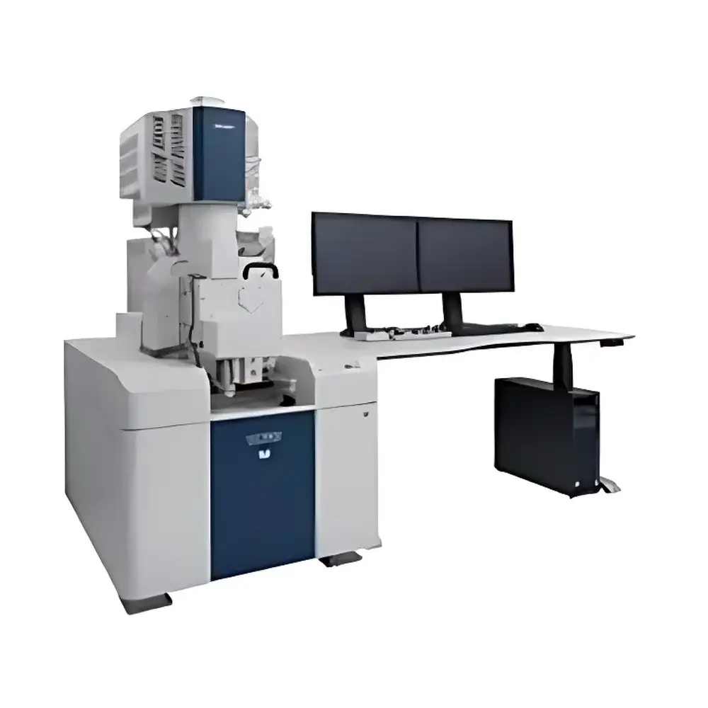
| Brand | Hitachi |
|---|---|
| Origin | Japan |
| Manufacturer | Hitachi High-Tech Corporation |
| Product Type | Imported Instrument |
| Model | SU7000 |
| Electron Gun | Cold Field-Emission (CFEG) |
| Secondary Electron (SE) Resolution | 0.8 nm @ 15 kV, 0.9 nm @ 1 kV |
| Magnification Range | 20× to 2,000,000× |
| Accelerating Voltage | 0.1–30 kV |
| Backscattered Electron (BSE) Resolution | Not Specified |
| Detector Channels | Simultaneous 6-channel signal acquisition and display |
| Maximum Image Resolution | 10240 × 7680 pixels |
| Sample Chamber | Ultra-large chamber with 18 accessory ports |
| Vacuum Mode | High vacuum and low vacuum (down to 300 Pa, optional) |
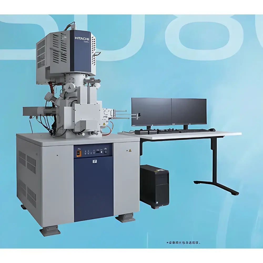
| Brand | Hitachi |
|---|---|
| Origin | Japan |
| Manufacturer | Hitachi High-Tech Corporation |
| Type | Floor-standing FE-SEM |
| Electron Source | Cold Field-Emission Gun |
| Secondary Electron Resolution | 0.6 nm @ 15 kV |
| Magnification Range | 20× – 2,000,000× |
| Accelerating Voltage | 0.5–30 kV (standard mode) |
| Backscattered Electron Resolution | Not specified |
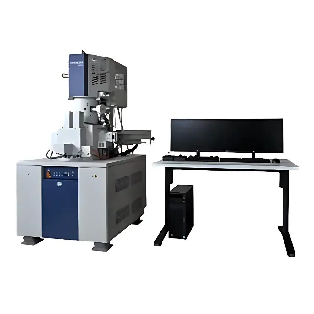
| Brand | Hitachi |
|---|---|
| Origin | Japan |
| Model | SU8600 Series |
| Instrument Type | Floor-Standing SEM |
| Electron Gun | Cold Field Emission |
| Secondary Electron Resolution | 0.6 nm @ 15 kV |
| Magnification Range | 20× to 2,000,000× |
| Accelerating Voltage | 0.5–30 kV |
| Landing Voltage | 0.01–20 kV |
| Maximum Sample Diameter | φ150 mm |
| Detector Options | UD (with ExB energy filter), LD, TD (with energy filter), IMD, PD-BSED, OCD, CLD, STEM Detector |
| Stage | 5-Axis Motorized (X: 0–110 mm, Y: 0–110 mm, Z: 1.5–40 mm, Tilt: −5° to +70°, Rotation: 360°) |
| Software | EM Flow Creator, HD Capture (up to 40,960 × 30,720 px) |
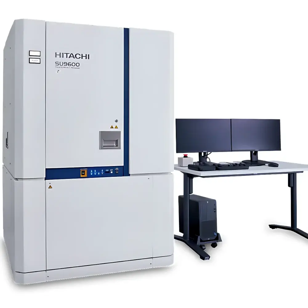
| Brand | Hitachi |
|---|---|
| Origin | Japan |
| Manufacturer | Hitachi High-Tech Corporation |
| Type | Floor-standing SEM |
| Electron Source | Schottky field-emission gun |
| Secondary Electron Resolution | 0.6 nm @ 15 kV, 0.8 nm @ 1 kV, 0.9 nm @ 0.3 kV |
| Magnification Range | 20× – 2,000,000× |
| Accelerating Voltage | 0.1–30 kV (standard mode) |
| Maximum Image Size (optional) | 40,960 × 30,720 pixels |
| Simultaneous Signal Channels | Up to 6 detectors |
| EDS Working Distance Optimization | Short WD configuration enabled via optimized chamber geometry |
| Brand | Hitachi |
|---|---|
| Origin | Japan |
| Manufacturer | Hitachi High-Tech Corporation |
| Type | Floor-Standing SEM |
| Electron Source | Cold Field-Emission Gun (CFEG) |
| Resolution | 0.6 nm @ 1 kV, 0.4 nm @ 30 kV (Secondary Electron Imaging) |
| Magnification Range | 80× to 3,000,000× |
| Accelerating Voltage | 0.01–30 kV |
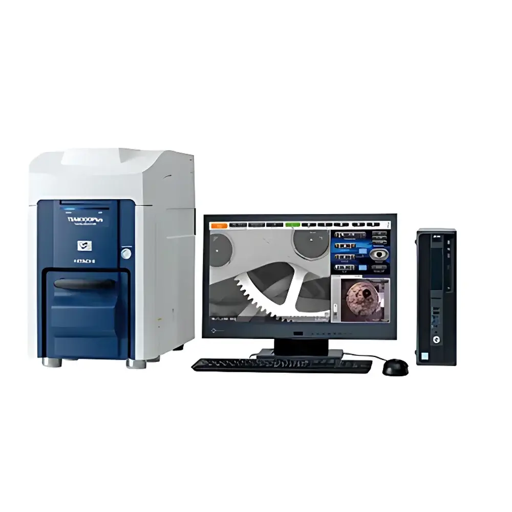
| Brand | Hitachi |
|---|---|
| Origin | Japan |
| Model | TM4000II / TM4000PlusII |
| Accelerating Voltage | 5 kV / 10 kV / 15 kV (4-step current adjustment per voltage) |
| Magnification Range | 10× to 100,000× |
| Detector Configuration | Quad-segment backscattered electron detector (BSE) |
| Sample Chamber Dimensions | Ø80 mm × 50 mm (max. height) |
| Imaging Modes | Conductive mode (TM4000PlusII), Standard mode, Charge-free mode |
| Software Features | SEM-MAP navigation, report-generation export (PDF/HTML), real-time BSE + SE image overlay (TM4000PlusII) |
| Camera Resolution | 2560 × 1920 (CCD) |
| EDS Compatibility | Integrated EDX interface |
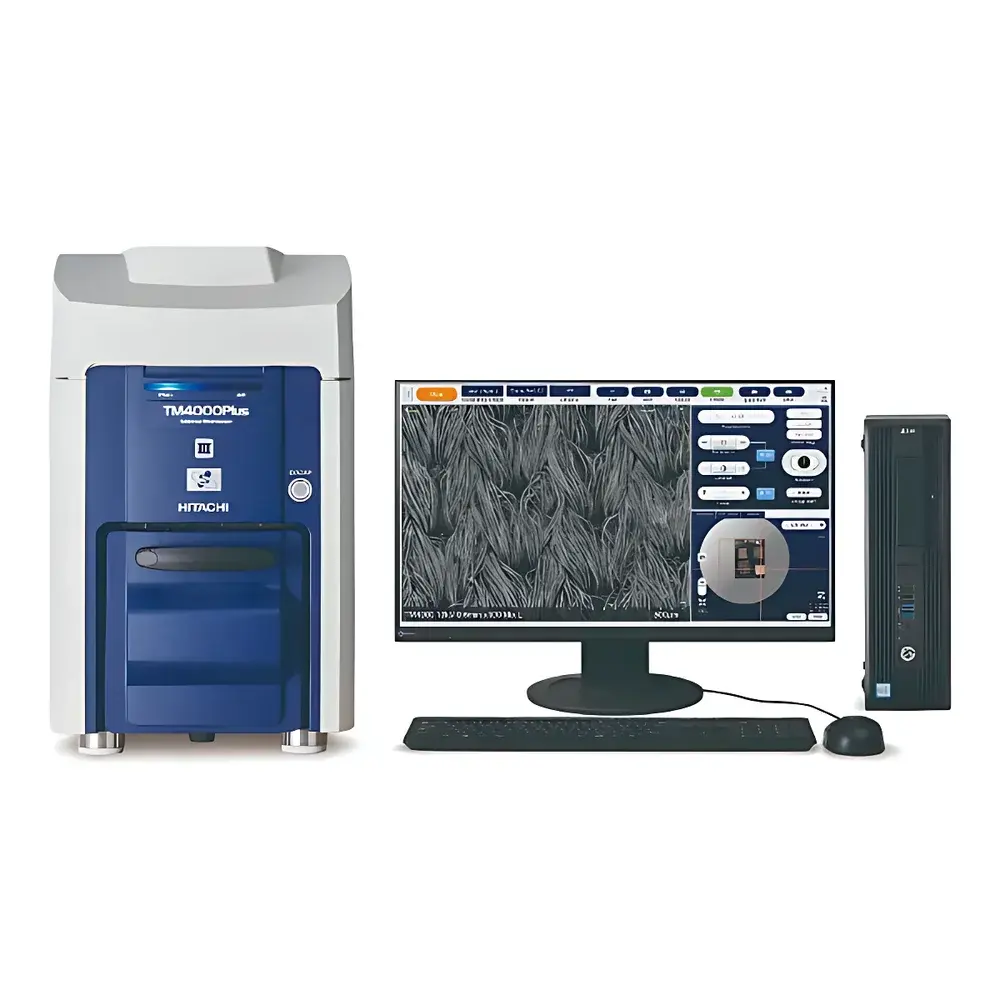
| Brand | Hitachi |
|---|---|
| Origin | Japan |
| Manufacturer Type | Original Equipment Manufacturer (OEM) |
| Product Category | Imported Instrument |
| Model | TM4000PlusIII / TM4000III |
| Instrument Type | Benchtop SEM |
| Electron Source | Tungsten Filament |
| Accelerating Voltage | 5 kV, 10 kV, 15 kV, 20 kV |
| Magnification Range | 10× – 100,000× (photographic magnification) |
| Maximum Sample Diameter | 80 mm |
| Maximum Sample Thickness | 50 mm |
| Stage Travel | X: 40 mm, Y: 35 mm |
| Vacuum Mode | Standard Low-Vacuum Operation |
| Automation Features | Auto-focus, Auto-brightness/contrast, Filament Usage Monitoring, Programmable Workflow Sequencing, Integrated Particle Analysis Support (with Oxford AZtecLiveLite) |
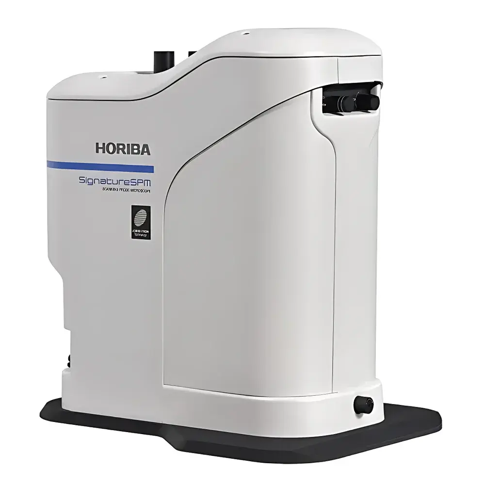
| Brand | HORIBA |
|---|---|
| Origin | France |
| Manufacturer Type | Manufacturer |
| Import Status | Imported |
| Model | Signature SPM |
| Instrument Category | Atomic Force Microscope |
| Instrument Type | Materials-Focused AFM |
| Spectroscopy Integration | Confocal Raman & Photoluminescence (PL) |
| Core Capability | True Co-Localized Multimodal Imaging (Topography + Nanomechanics + Electrostatics + Magnetism + Chemical Fingerprinting) |
| Scanner Range | 100 × 100 × 15 µm |
| Optical Access | Dual-Path, IR AFM Laser (1310 nm) + Visible/NIR Excitation Lasers (e.g., 532 nm, 638 nm, 785 nm) |
| Spectrometer | Achromatic, >95% Reflectivity, Triple-Grating Support (150–6000 cm⁻¹) |
| Software Feature | “Probe Away” / “Probe Back” Automated Tip Retraction & Re-Registration |
| Compliance | Designed for GLP/GMP-adjacent research environments |
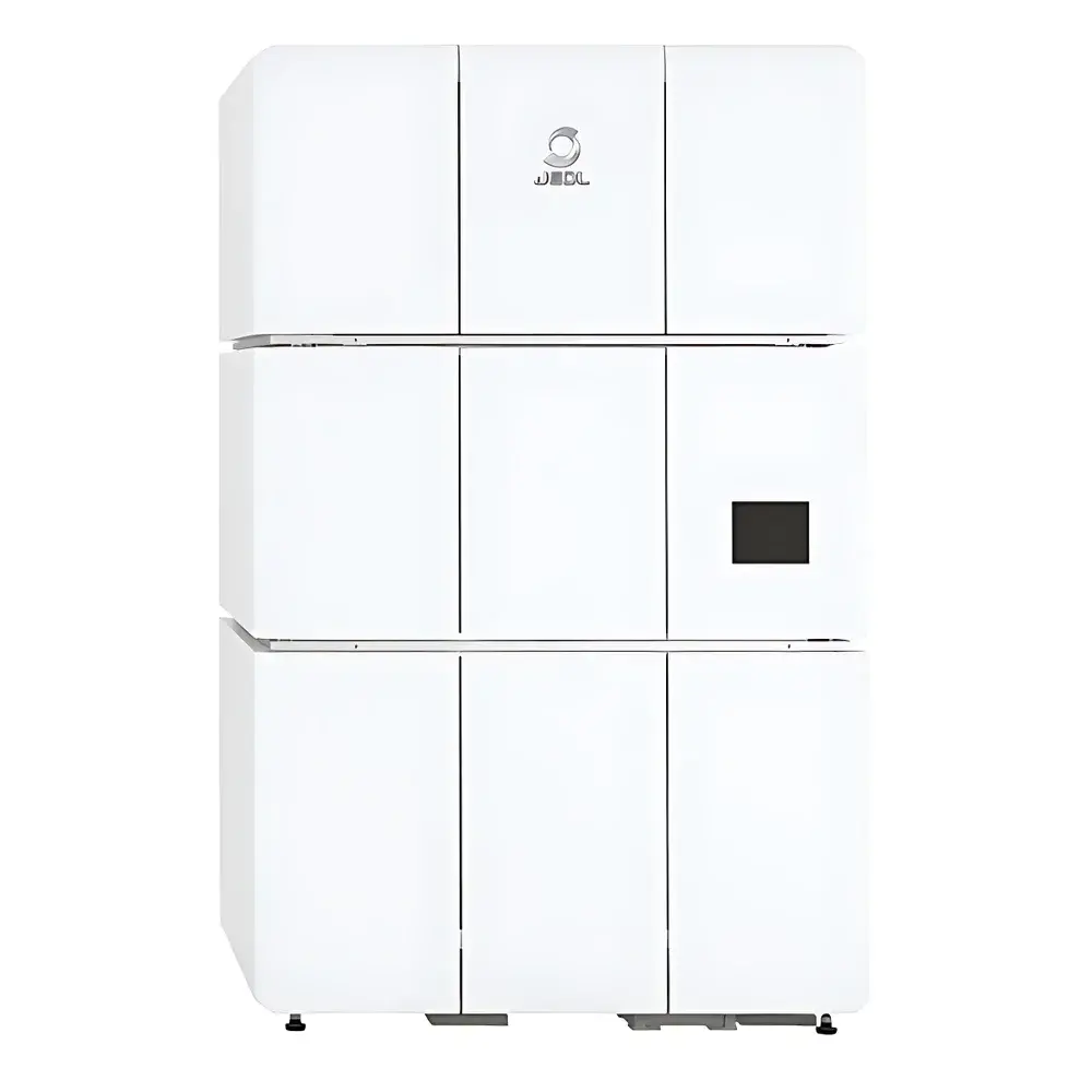
| Brand | JEOL |
|---|---|
| Origin | Japan |
| Model | CRYO ARM™ 200 II (JEM-Z200CA) |
| Acceleration Voltage | 200 kV |
| Magnification Range | ×100 to ×1,000,000 |
| Spherical Aberration Coefficient (Cs) | 1.5 mm |
| Chromatic Aberration Coefficient (Cc) | 1.8 mm |
| Specimen Temperature | ≤100 K |
| Sample Storage Capacity | Up to 12 cryo-samples |
| Energy Filter | Integrated Omega-type Energy Filter |
| Optional Software | JEOL Automated Data Acquisition System (JADAS) |
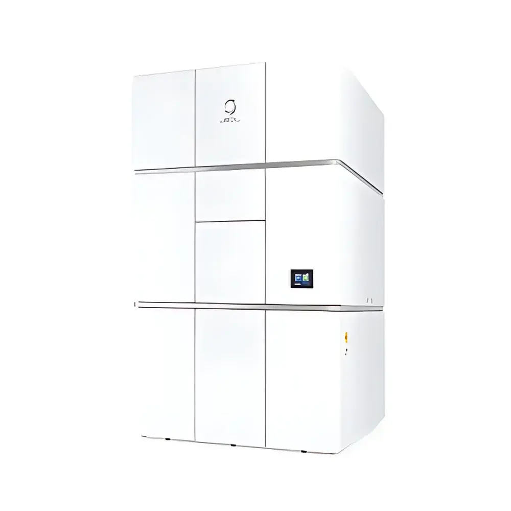
| Brand | JEOL |
|---|---|
| Origin | Japan |
| Manufacturer Type | Authorized Distributor |
| Origin Category | Imported |
| Model | JEM-3300 |
| Price Range | USD 6.2–6.9 million (est.) |
| Acceleration Voltage | Up to 300 kV |
| Magnification Range | 2,000× – 1,000,000× |
| Electron Source | Cold Field Emission Gun (CFEG) |
| Energy Filter | Integrated Omega-Type Electron Energy Filter |
| Automation | Automated Sample Loading System, JADAS Software Suite, Phase Plate Compatibility, Köhler Illumination Optics |
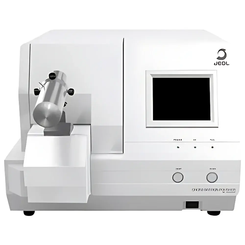
| Brand | JEOL |
|---|---|
| Origin | Japan |
| Model | IB-19530CP |
| Price | USD 150,000 |
| Equipment Type | Ion Beam Sample Preparation System for Electron Microscopy |
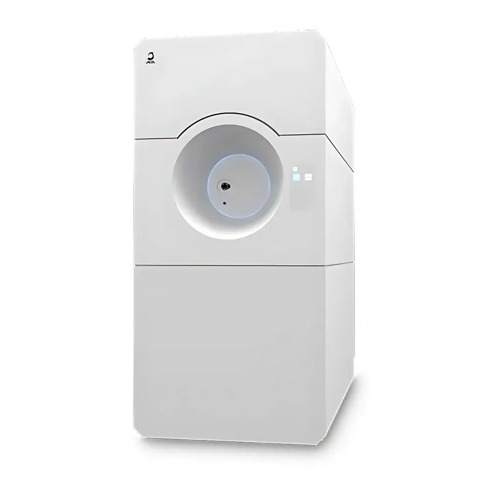
| Brand | JEOL |
|---|---|
| Origin | Japan |
| Manufacturer Type | Authorized Distributor |
| Product Origin | Imported |
| Model | JEM-120i |
| Acceleration Voltage | Up to 120 kV |
| Magnification Range | 50× – 1,200,000× |
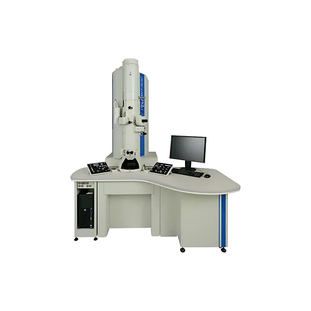
| Brand | JEOL |
|---|---|
| Origin | Japan |
| Model | JEM-2100Plus |
| Acceleration Voltages | 80, 100, 120, 160, 200 kV |
| Magnification Range | 50× to 1,500,000× |
| Point Resolution | 0.19 nm |
| Line Resolution | 0.14 nm |
| Minimum Probe Size | 0.5 nm |
| Tilt Range | ±25° |
| Condenser System | Three-Stage Lens Design |
| Pole Piece Options | UHR, HR, HT, HC, CRYO |
| Operating System | 64-bit Windows-based Control Interface |
| Integrated Detectors | STEM, EDS, CCD, EELS |
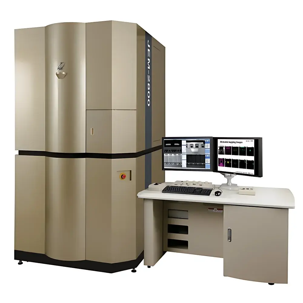
| Brand | JEOL |
|---|---|
| Origin | Japan |
| Model | JEM-2800 |
| Point Resolution | 0.21 nm |
| Lattice Resolution | 0.10 nm |
| STEM Resolution | 0.16 nm |
| Secondary Electron Resolution | 0.5 nm |
| EDS Configuration | Dual Ultra-High-Sensitivity Silicon Drift Detectors (SDD) |
| Lorentz Mode | Standard Equipment |
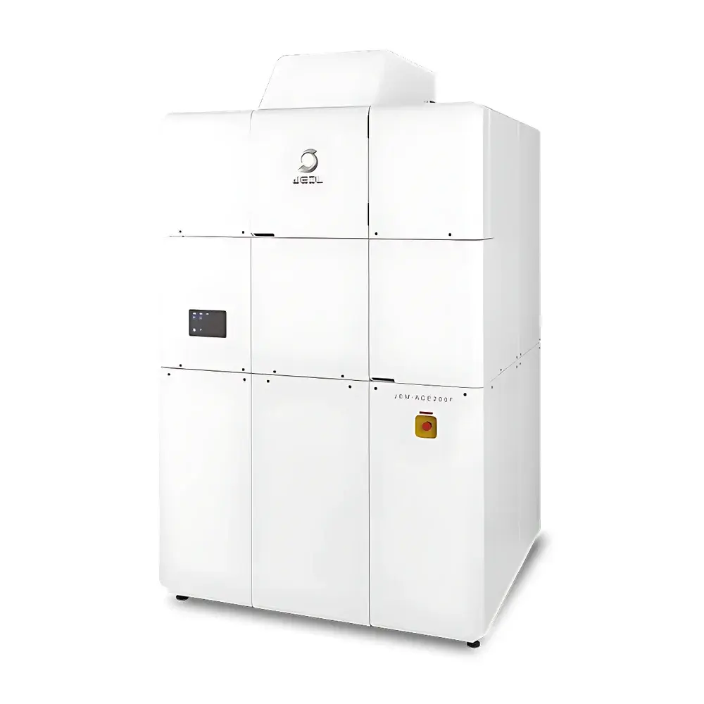
| Brand | JEOL |
|---|---|
| Origin | Japan |
| Manufacturer Type | Authorized Distributor |
| Product Origin | Imported |
| Model | JEM-ACE200F |
| Price | USD $3,000,000 |
| Acceleration Voltage | Up to 200 kV |
| Maximum Magnification | 2,000,000× |
| Point Resolution | 0.21 nm |
| Lattice Resolution | 0.10 nm |
| STEM Resolution | 0.136 nm |
| Information Limit | 0.11 nm |
| EDS Configuration | Dual Ultra-High-Sensitivity Silicon Drift Detectors (SDD) |
| Lorentz Mode | Standard |