
Electron Microscope
Filter
Showing 211–240 of 442 results
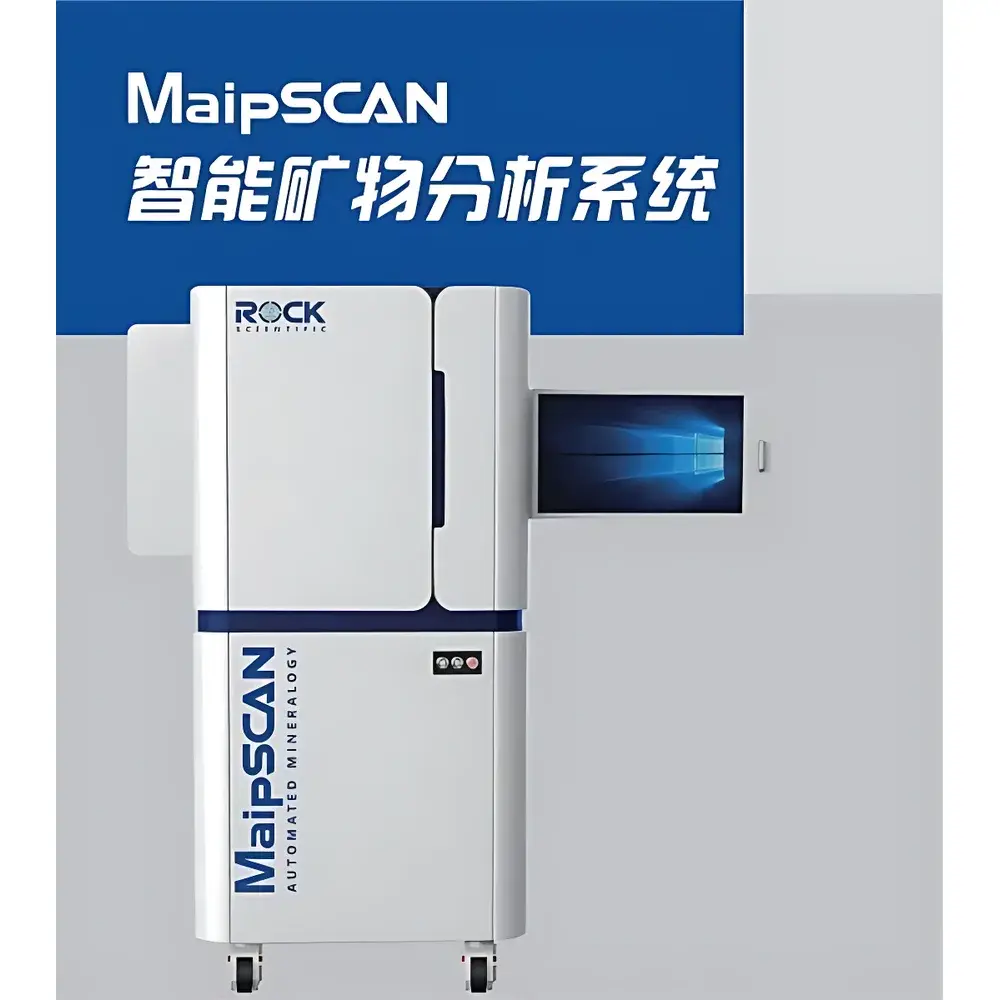
| Brand | ROCK |
|---|---|
| Origin | Hong Kong, China |
| Model | MaipSCAN |
| Instrument Type | Floor-standing SEM |
| Electron Source | Tungsten Filament |
| Secondary Electron Resolution | 3.0 nm @ 30 kV (SE and W) |
| Magnification Range | 7× – 1,000,000× |
| Accelerating Voltage | 0.2 – 30 kV |
| Backscattered Electron Resolution | 4.0 nm @ 30 kV (VP mode with BSD) |
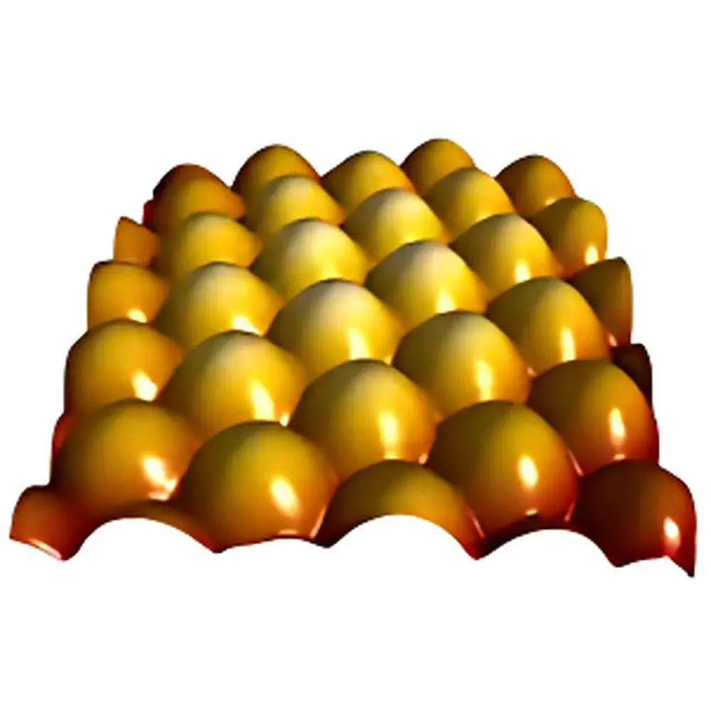
| Brand | MCL Think Nano |
|---|---|
| Origin | USA |
| Manufacturer Type | Authorized Distributor |
| Import Status | Imported |
| Model | MadPLL® |
| Price Range | USD $14,000 – $72,000 (based on configuration) |
| Positional Detection Noise | 0.15 nm RMS |
| Sample Diameter Limit | <15 mm |
| XY Scan Range (with compatible stages) | up to 200 µm |
| Z-Range (with Nano-OP30) | 30 µm (closed-loop), 100 µm (open-loop) |
| PLL Frequency Lock Range | 10–100 kHz |
| Phase Shift Resolution | <0.1° |
| Demodulation Bandwidth | 3 kHz |
| PCC Compensation Range | ±50 pF |
| Operating Systems | Windows 7/10/11 (32/64-bit), LabVIEW 2015+ compatible |
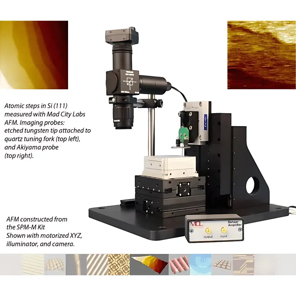
| Brand | MCL Think Nano |
|---|---|
| Origin | USA |
| Model | SPM-M Kit |
| Detection Noise | <0.15 nm RMS |
| Sample Size | <15 mm |
| XY Scan Range | 200 × 200 µm |
| Z Positioning | Nano-OP30 (closed-loop optional) |
| Controller | 3-Axis Nano-Drive® with PicoQ® sensors |
| Probe Options | Quartz tuning forks (5 included), Akiyama probe boards, tungsten tip etching compatibility |
| Software | AFMView™ with automated PLL control |
| Compliance | Designed for GLP/GMP-aligned research environments |
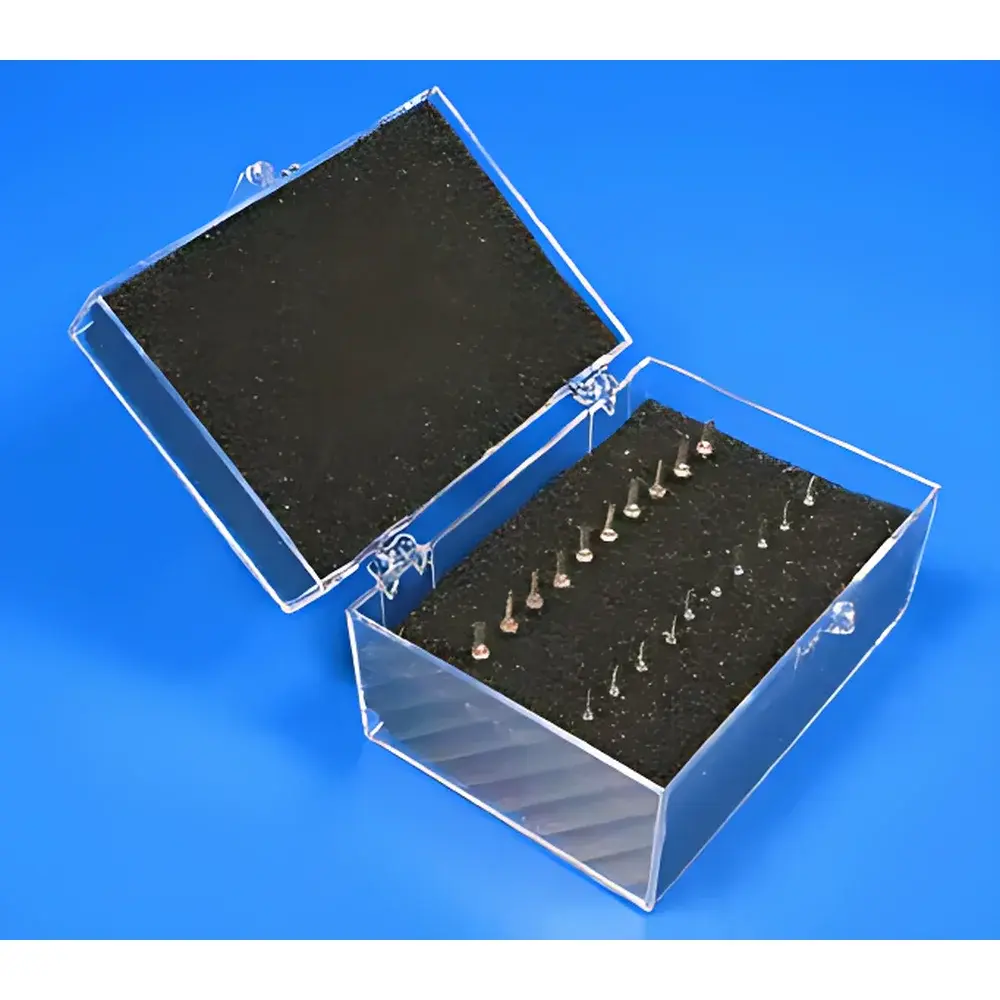
| Brand | MCL Think Nano |
|---|---|
| Origin | USA |
| Model | Tuning Forks |
| Center Frequency | 32.768 kHz |
| Oscillation Mode | Fundamental |
| Series Resistance (max.) | 30 kΩ |
| Tolerance (at 25 °C) | ±18 ppm |
| Operating Temperature Range | −10 °C to +60 °C |
| Frequency Stability Over Temperature | −0.038 ppm/°C |
| Drive Level | 10 µW |
| Shunt Capacitance (max.) | 1.7 pF |
| Motional Capacitance | 2.5 fF |
| Load Capacitance | 12.5 pF |
| Aging (max.) | ±3 ppm/year |
| Packaging | Pre-cleaned, “out-of-the-can” ready-to-mount configuration |
| Available Sizes | Medium and Large |
| Brand | MCL Think Nano |
|---|---|
| Origin | USA |
| Manufacturer Type | Authorized Distributor |
| Origin Category | Imported |
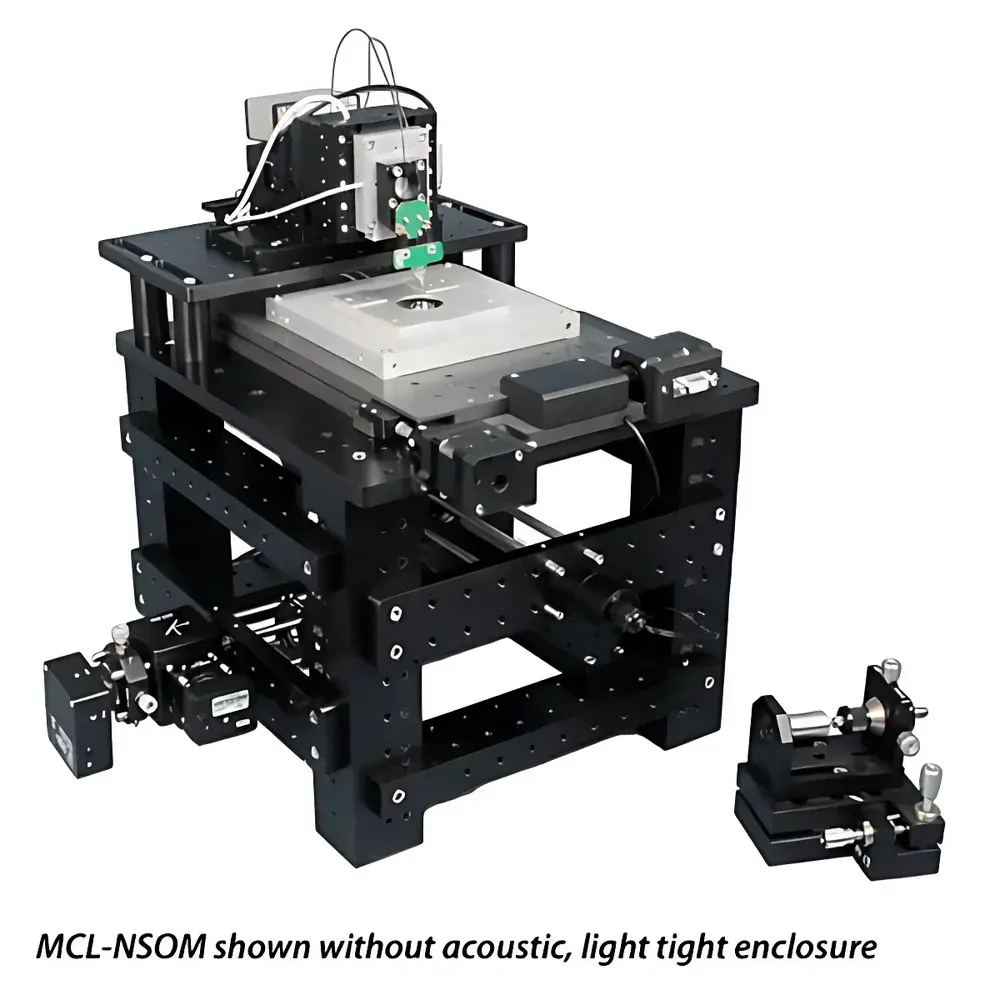
| Model | MCL-NSOM |
| Instrument Type | Materials-Focused NSOM System |
| Positioning Noise | X-Y ≤ 0.15 nm RMS, Z = 35 pm RMS |
| Typical Imaging Bandwidth | 625 Hz |
| Sample Dimensions | Ø ≤ 15 mm, Thickness ≤ 5 mm |
| Sample Stage Travel Range | Ø ≤ 15 mm, Thickness ≤ 5 mm |
| XY Micropositioner Range | 25 mm |
| Z Lens Micropositioner Range | 50 mm |
| Fiber XYZ Micropositioner Range | 25 mm |
| Micropositioner Step Size | 95 nm |
| Piezo Nanopositioner Range (XYZ) | 200 µm × 200 µm × 30 µm |
| Piezo Resolution | 0.4 nm (XY), 0.06 nm (Z) |
| Piezo Step Size | 0.2 nm (XY), 0.03 nm (Z) |
| Excitation Source | 635 nm, 5 mW laser diode with fiber coupling |
| Objective | 20× oil immersion, 0.4 NA, infinity-corrected |
| Detection | Avalanche photodiode (200–1000 nm, 1 mm active area) |
| Alignment Camera | 0.3 MP CMOS |
| Feedback Mode | Shear-force |
| NSOM Modes | Illumination, Collection, Illumination+Collection, Reflection, Reflection+Collection |
| Control Software | AFMView™ and LabVIEW™-based automation suite |
| Controller Interfaces | USB 2.0, 20-bit DAC/ADC, 4-channel TTL I/O |
| Operating System Compatibility | Windows Vista/7/8/10 |
| Brand | Mel-Build |
|---|---|
| Origin | Japan |
| Manufacturer Type | Authorized Distributor |
| Origin Category | Imported |
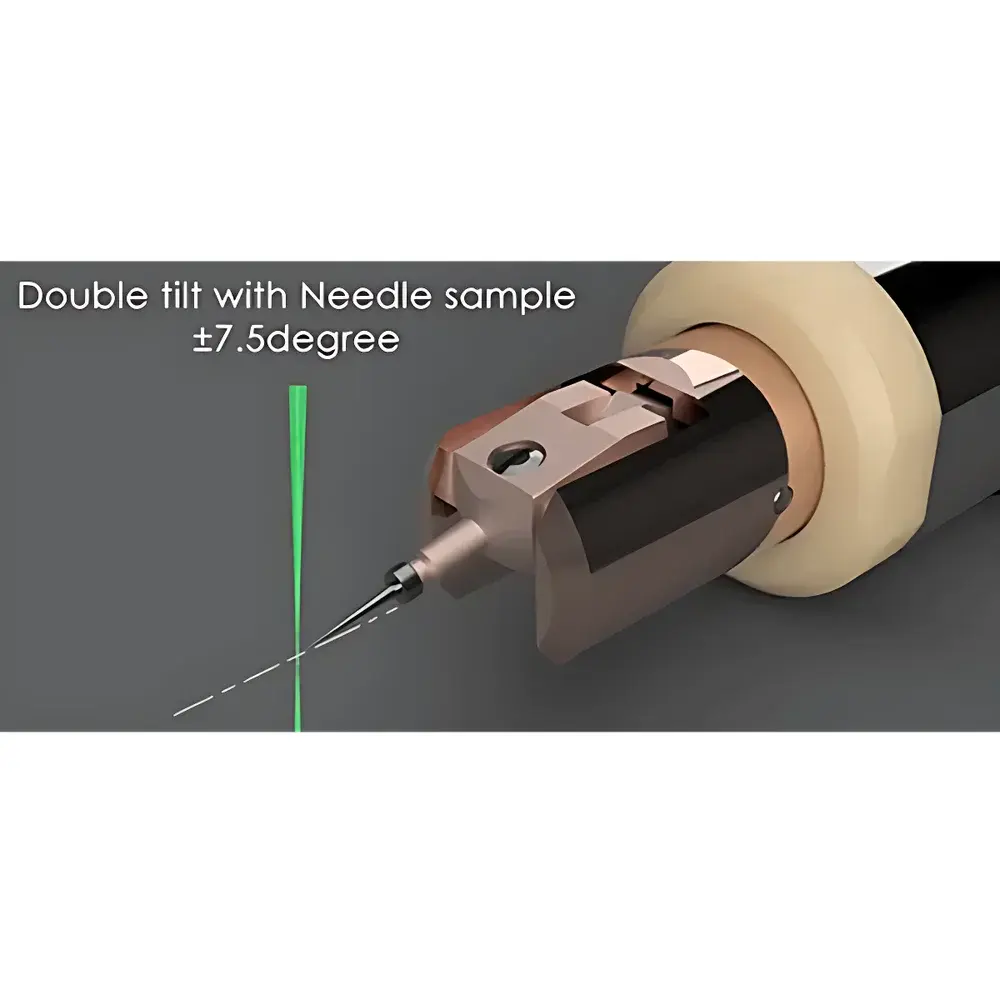
| Model | Dual-Tilt Probe TEM Sample Holder |
| Pricing | Available Upon Request |
| Brand | Quantum Detectors |
|---|---|
| Origin | United Kingdom |
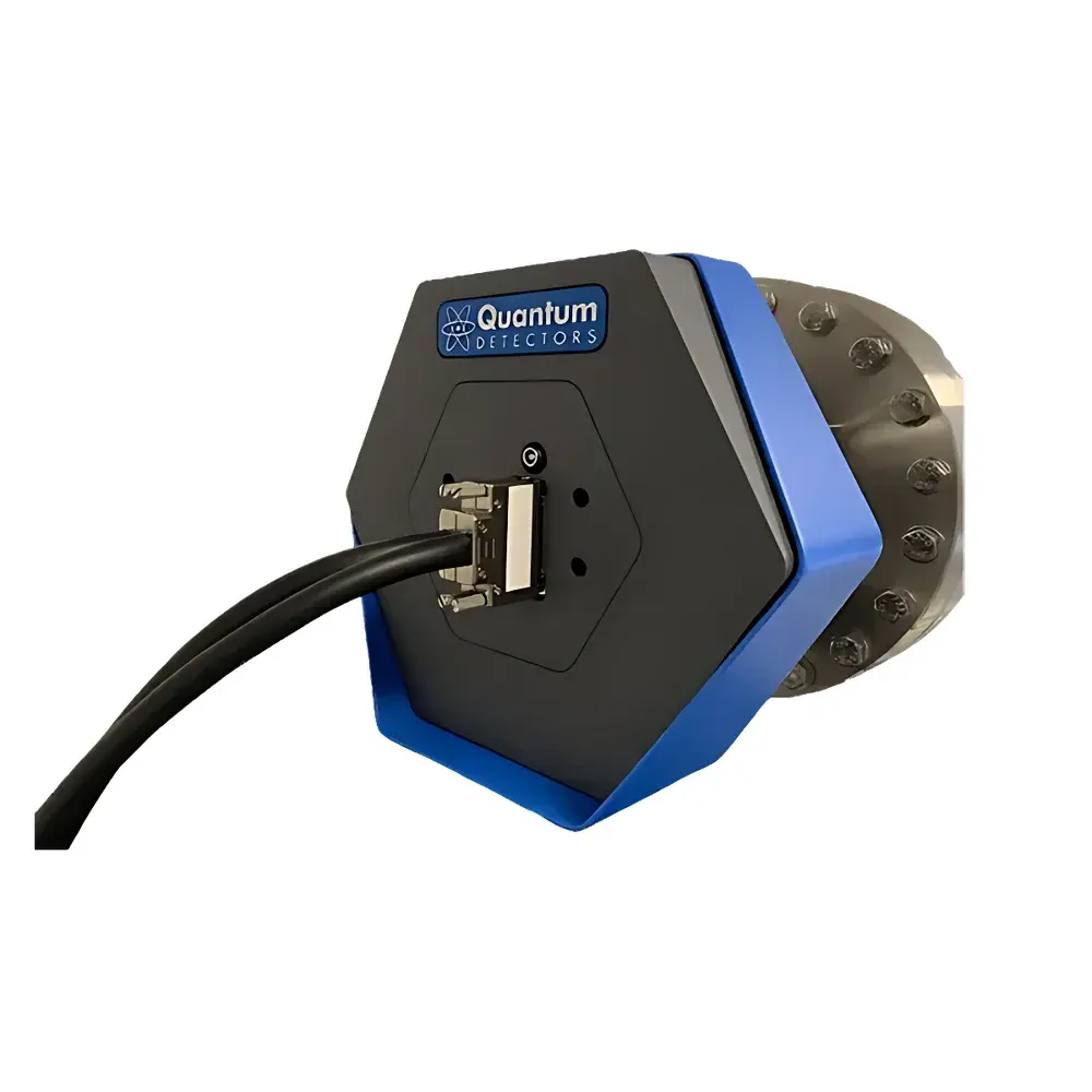
| Model | MerlinEELS |
| Detector Architecture | Hybrid Pixel (4 × Medipix3 RX chips) |
| Format | 1024 × 256 pixels |
| Frame Rate | up to 3600 fps (6-bit mode, full frame) |
| Dynamic Range | >16 million counts per pixel |
| Readout Noise | 0 e⁻ rms |
| Dead Time | 0 ns (dual counter per pixel) |
| Pixel Size | 55 µm |
| Energy Thresholding | User-configurable single-electron discrimination |
| ROI Modes | 4–128 rows selectable (N × 256 px) |
| Integration | TEM-compatible with dedicated scan generator and multi-signal synchronization |
| Brand | MicroInno |
|---|---|
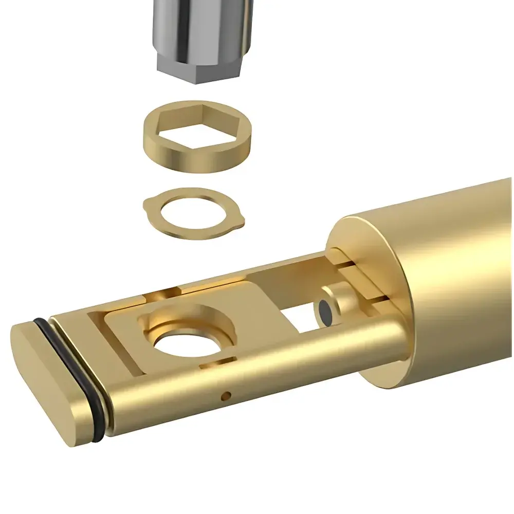
| Model | MIVTHD-TF/JL |
| Compatibility | Thermo Fisher, JEOL, Hitachi TEMs |
| Dual-Axis Tilt Range | α/β ±30° (typ.) |
| Tilt Resolution | < 0.1° |
| Linear Translation Resolution | < 1.5 nm/min |
| Sealing Mechanism | Retractable Viton O-ring |
| Sample Mounting | Hex-screw clamping |
| Vacuum Compatibility | ≤1×10⁻⁷ Pa |
| Gas Environment | Inert gas (Ar/N₂) or high vacuum transfer |
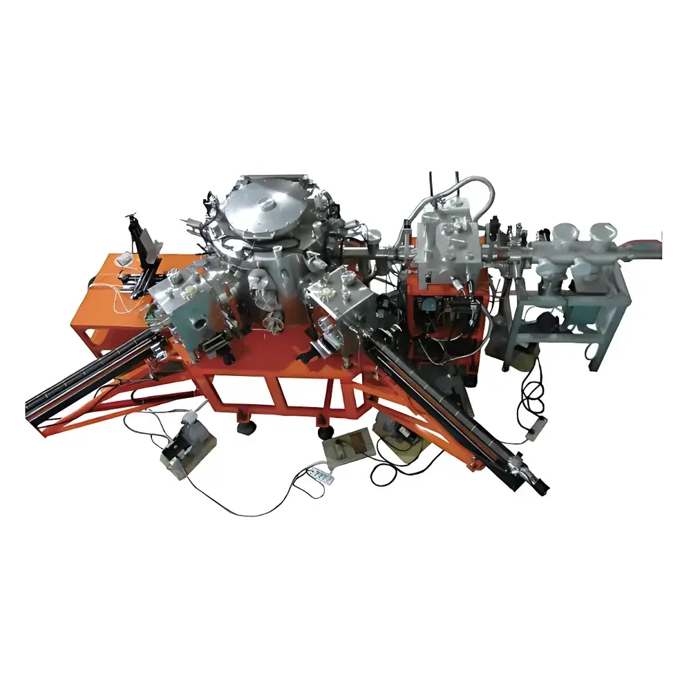
| Brand | Makeway |
|---|---|
| Model | MKW-3000 |
| Origin | Shanghai, China |
| Detector Type | Multi-probe EDS-compatible |
| Energy Resolution | 120 eV |
| Operating Environments | High Vacuum & Ambient Air |
| Maximum Beam Scan Area | 60 × 60 mm² |
| Sample Positioning | 4-axis Motorized Stage (Vacuum & Air) |
| Beam Control | Motorized Variable Aperture & Remote Focusing |
| Compliance | Designed for ISO/IEC 17025-aligned radiation effects testing workflows |
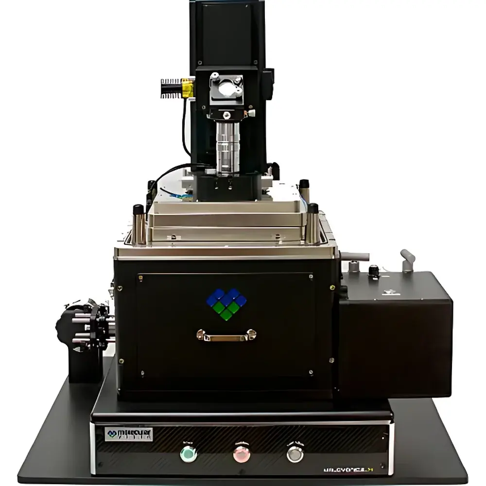
| Brand | Molecular Vista |
|---|---|
| Origin | USA |
| Model | Vista-SNOM |
| Positioning Detection Noise | ≤ 50 pm RMS |
| Sample Size | Ø ≤ 25 mm, Thickness ≤ 10 mm |
| Sample Stage Travel Range | 6 mm × 6 mm |
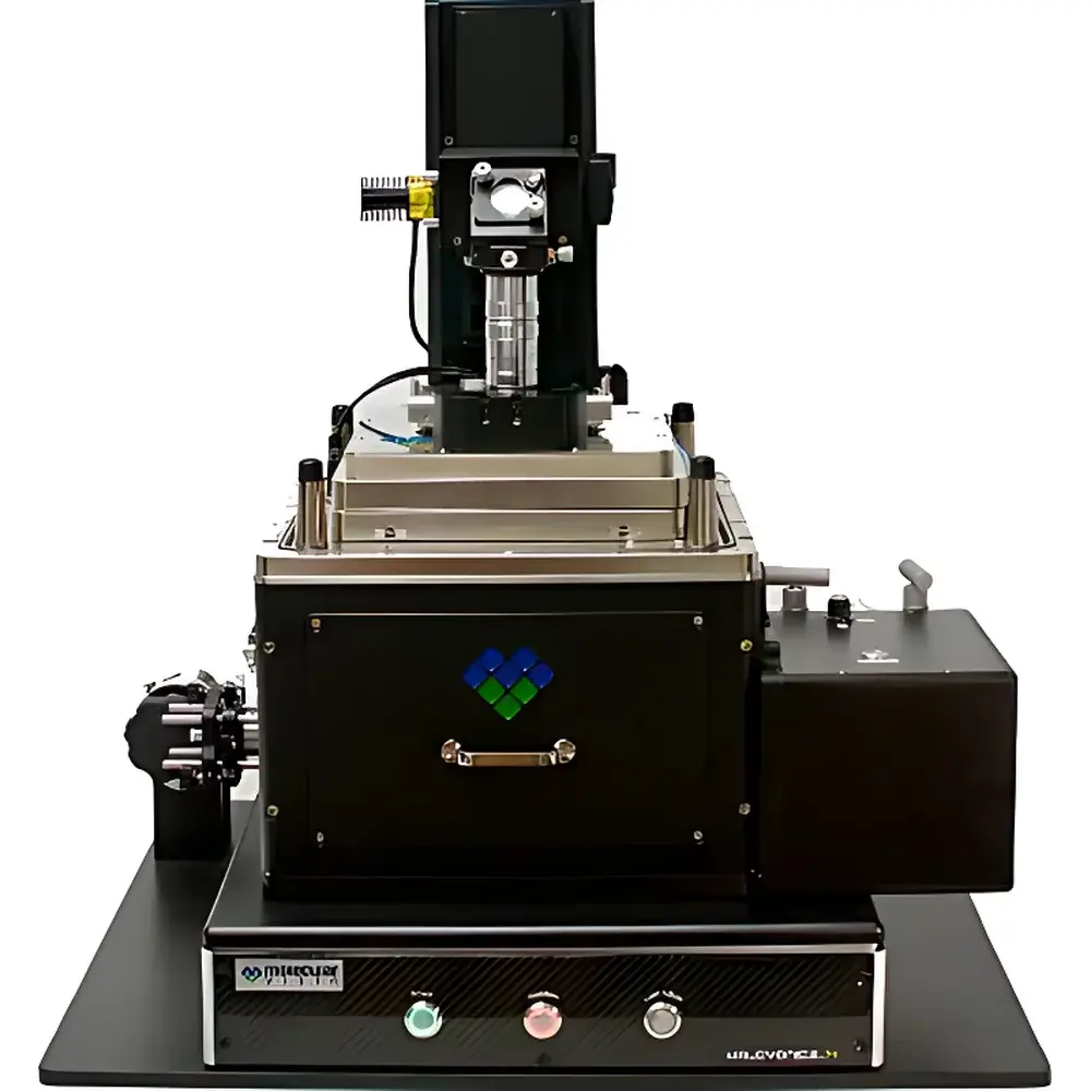
| Brand | Molecular Vista |
|---|---|
| Origin | USA |
| Manufacturer Type | Authorized Distributor |
| Origin Category | Imported |
| Model | VistaScope |
| Price Range | USD 420,000 – 700,000 |
| Instrument Type | Material Science AFM |
| Position Detection Noise | ≤ 50 pm RMS |
| Sample Dimensions | Ø ≤ 25 mm, Thickness ≤ 10 mm |
| XY Stage Travel Range | 6 mm × 6 mm |
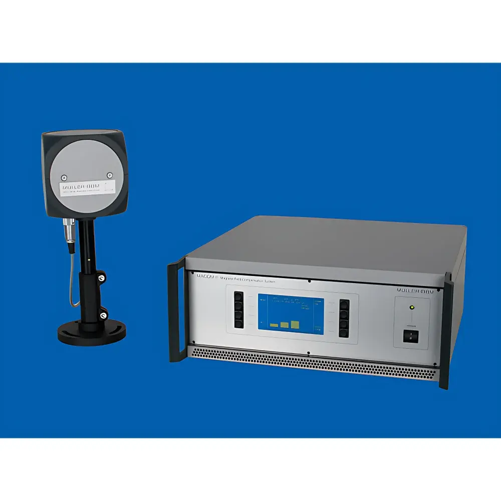
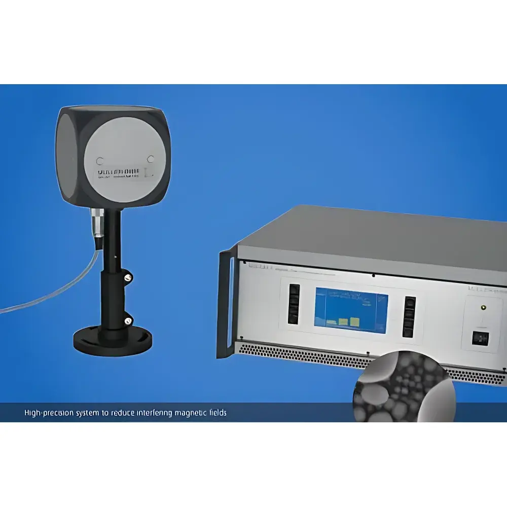
| Brand | Müller-BBM |
|---|---|
| Origin | Germany |
| Model | MACOM II |
| Operating Frequency Range | 0 Hz to 50 kHz |
| Control Interface | Ethernet / TCP/IP |
| Display | Integrated LCD with real-time monitoring and parameter adjustment |
| Remote Operation | Supported via internal network or internet (optional global remote support) |
| Compliance | Designed for integration with TEM/SEM, e-beam lithography, and MRI systems requiring ultra-low magnetic noise environments |
| Maintenance | Minimal — no consumables or routine calibration required |
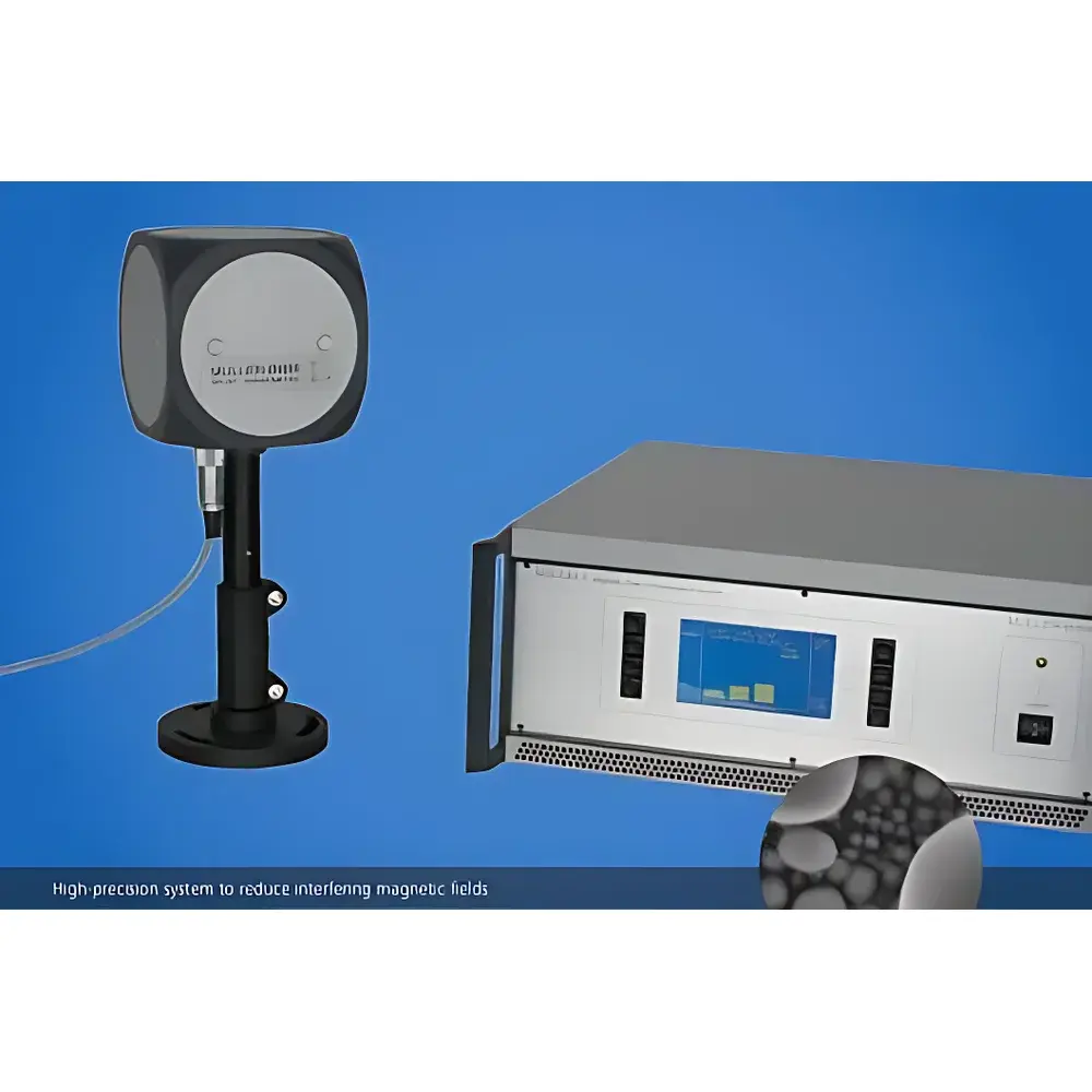
| Brand | Müller-BBM |
|---|---|
| Origin | Germany |
| Model | MACOM II® |
| Frequency Range | 0 Hz – 50 kHz |
| Operating Axes | 3-axis (X, Y, Z) |
| Interface | RS-232 serial + Ethernet (TCP/IP) |
| Display | Integrated LCD for real-time monitoring of residual field & coil current per axis |
| Compliance | Designed for GLP/GMP-adjacent environments |
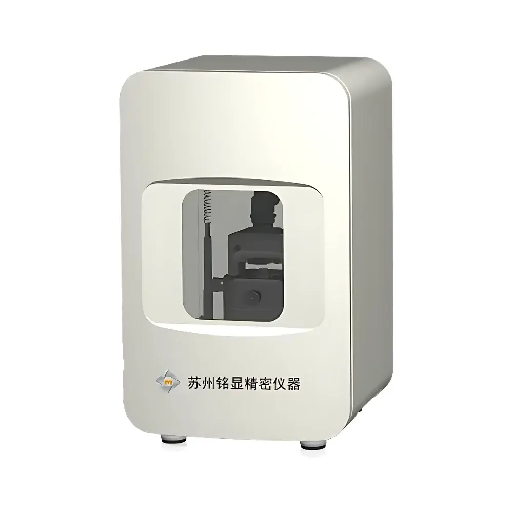
| Brand | MULLER-BBM |
|---|---|
| Origin | Germany |
| Model | MACOM II® |
| Frequency Range | 0 Hz to 50 kHz |
| Operating Axes | 3-axis (X, Y, Z) |
| Interface | RS-232 serial + Ethernet (TCP/IP) |
| Display | Integrated LCD for real-time monitoring and parameter adjustment |
| Control | Local front-panel + remote via LAN/internet |
| Maintenance | Maintenance-free after commissioning |
| Compliance | Designed for GLP/GMP-adjacent environments |
| Brand | MX-AFM |
|---|---|
| Origin | Jiangsu, China |
| Manufacturer Type | Authorized Distributor |
| Country of Origin | China |
| Model | MX-plorer Premium |
| Instrument Type | Atomic Force Microscope (AFM) |
| Position Detection Noise | ≤ 50 pm |
| XY Sample Stage Travel Range | ≥ 5 mm |
| Operating Modes | Contact, Tapping, Phase Imaging, Conductive AFM (C-AFM), Kelvin Probe Force Microscopy (KPFM), Force Spectroscopy, Nanolithography |
| Control Architecture | Closed-Loop Piezoelectric Scanning System |
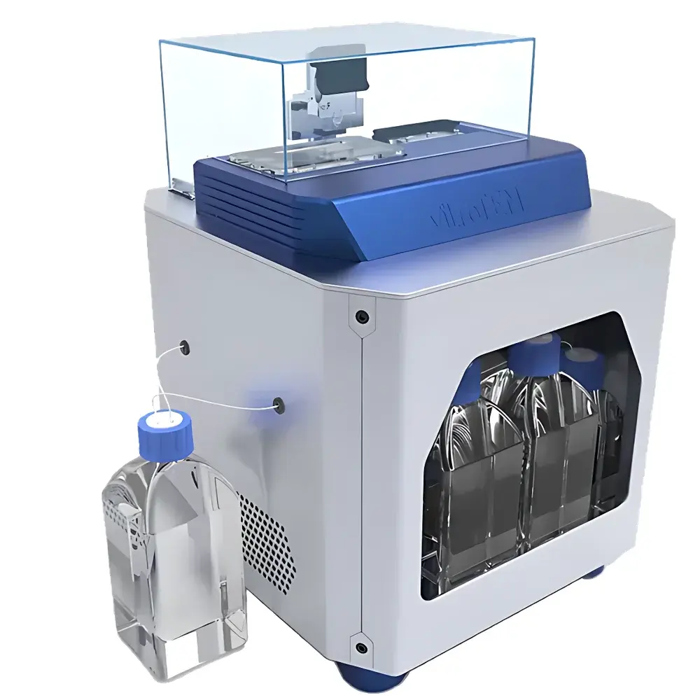
| Brand | VitroTEM |
|---|---|
| Origin | Netherlands |
| Manufacturer Type | Authorized Distributor |
| Product Origin | Imported |
| Model | Naiad |
| Pricing | Available Upon Request |
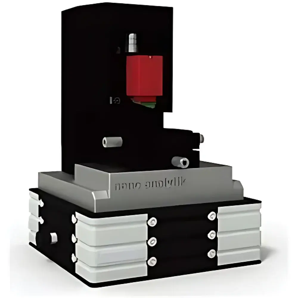
| Brand | Nano analytik |
|---|---|
| Origin | Germany |
| Model | AFM Series (SmartProbe Platform) |
| Instrument Type | Atomic Force Microscope |
| Vertical Position Detection Noise | 0.01 nm RMS |
| Maximum Sample Diameter | ≤10 cm |
| Scanner Range (Adeona) | 15 µm × 15 µm × 4 µm |
| Dimensions (Vacuum-Compatible Version) | 140 mm × 100 mm × 60 mm |
| Integrated Actuation & Sensing | Piezoresistive readout + bimaterial excitation on SmartProbe |
| XYZ Nanopositioning Range (Vacuum Variant) | 20 µm × 10 µm × 10 µm |
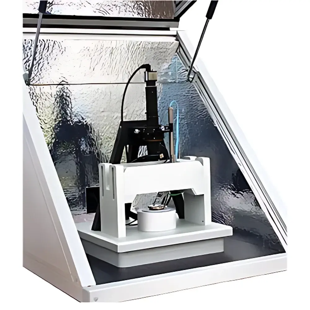
| Brand | Nano analytik |
|---|---|
| Origin | Germany |
| Model | SPL |
| Instrument Type | Atomic Force Microscope-based Scanning Probe Lithography System |
| Positioning Detection Noise | 0.01 nm (X, Y, Z) |
| Maximum Sample Diameter | 150 mm (6 in) |
| Stage Travel Range | 18 mm × 18 mm (expandable to 150 mm × 150 mm) |
| Minimum Feature Size | 5 nm (verified) |
| Direct-Write Speed | 300 µm/s |
| Overlay Accuracy | < 7 nm |
| Stitching Accuracy | < 10 nm |
| Maximum Writing Area per Field | 200 µm × 200 µm |
| Footprint | 80 cm × 100 cm × 190 cm |
| AFM Imaging Range | 10 µm × 10 µm × 5 µm (expandable to 200 µm × 200 µm) |
| Vertical RMS Noise | 0.01 nm |
| Closed-Loop Scan Linearity | 99.7% |
| Real-Time FPGA Feedback Bandwidth | 8 MHz |
| Data Acquisition Resolution | 16-bit (amplitude/phase) |
| Output Formats | BMP, PNG, JPG, TXT |
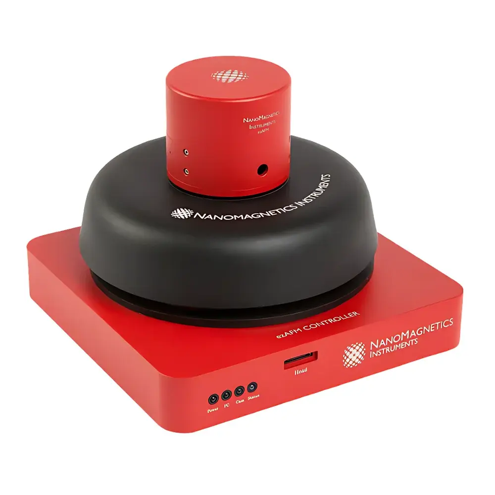
| Brand | NanoMagnetics |
|---|---|
| Origin | United Kingdom |
| Model | ezAFM |
| Instrument Type | Material-Grade AFM |
| Position Detection Noise | 75 fm/√Hz |
| Maximum Sample Dimensions | 10 × 10 × 5 mm |
| XY Stage Travel Range | 38 × 38 mm |
| Scan Areas | 120 × 120 × 40 µm (Z resolution: 0.2 nm) or 40 × 40 × 4 µm (Z resolution: 0.02 nm) |
| Lateral Resolution | 16 nm (large scan) / 5 nm (high-res scan) |
| Optical View System | Full HD CCD, 2 µm resolution, 390 × 230 µm FOV, 2516 × 1960 pixels, 30 fps |
| Controller | 24-bit ADC/DAC, FPGA/DSP-based digital feedback |
| Standard Imaging Modes | Contact, Tapping, Phase, LFM, MFM |
| Extended Modes (ezAFM+) | EFM, KPFM, C-AFM, SSRM, PRFM, FMM, nanomechanical mapping, liquid-phase, vacuum-compatible configurations |
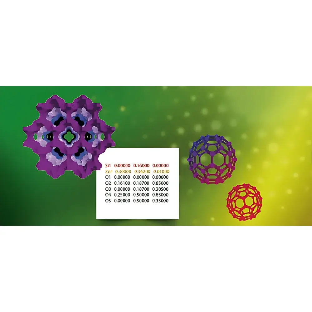
| Brand | NanoMEGAS |
|---|---|
| Origin | Belgium |
| Model | ADT-3D |
| Compatible TEM Voltage | 120–300 kV |
| Compatible Sources | LaB6, W, FEG |
| Minimum Crystal Size (Organic) | ~100 nm |
| Minimum Crystal Size (Inorganic) | ~20 nm |
| Tilt Range (Cell Parameter Determination) | −15° to +15°, 1° step |
| Recommended Tilt Range (Structure Solution) | −45° to +45°, 1° step or continuous rotation (MicroED) |
| Data Acquisition Modes | Manual or automated PED |
| Detector Compatibility | CCD cameras ≥1k × 1k resolution |
| Sample Holder Support | Single-tilt, tomography, cryo holders |
| Output | 3D reciprocal space reconstruction, unit cell parameters (2–5% error), space group assignment, integrated 3D reflection intensities |
| Compliance | Fully compatible with standard TEM workflows under GLP-aligned data handling practices |

| Brand | NanoMEGAS |
|---|---|
| Origin | Belgium |
| Model | ASTAR® |
| Compatibility | 120–300 kV TEM (including Cs-corrected FEG-TEM) |
| Spatial Resolution | 1–4 nm (FEG-TEM), <10 nm (LaB₆ TEM) |
| Acquisition Speed | Up to >1000 fps (with direct electron detectors) |
| PED Tilt Angle Range | 0.2°–2.5° |
| Output Data Types | Orientation Maps, Phase Maps, Correlation Index, Confidence Index, Virtual BF/DF Images, Grain Boundary Networks, Pole Figures, Strain-Compatible Integration (with TopSPIN) |
| Compliance | Fully compatible with GLP/GMP workflows requiring audit trails |
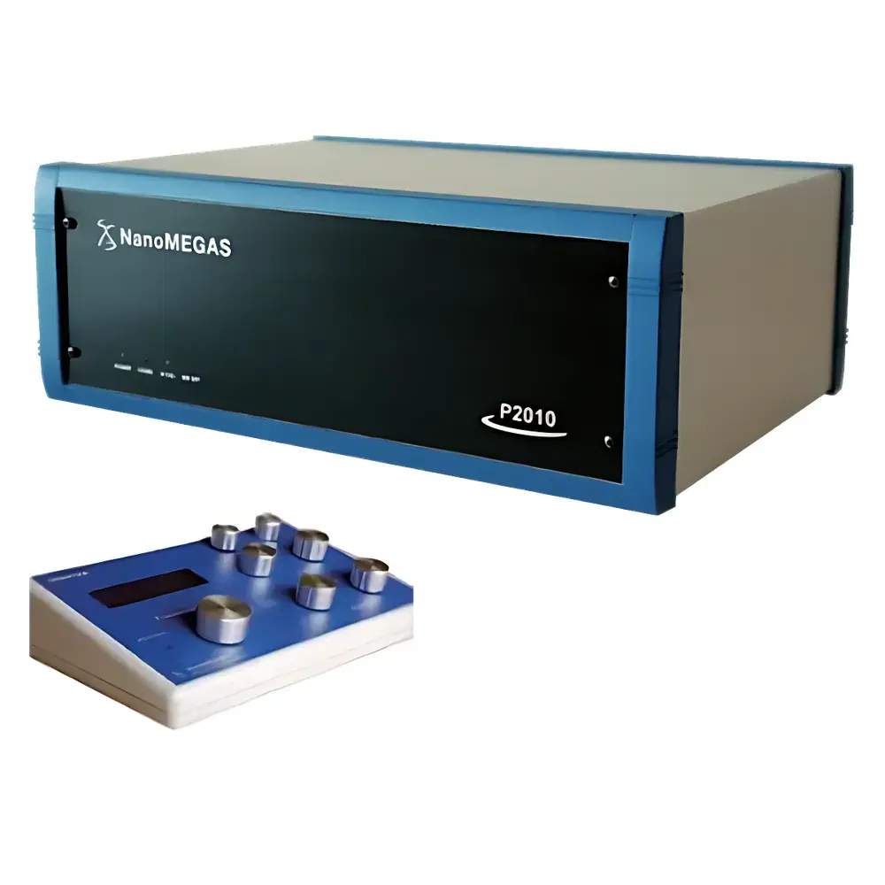
| Brand | NanoMEGAS |
|---|---|
| Origin | Imported (Non-China) |
| Manufacturer Type | Authorized Distributor |
| Model | DigiSTAR |
| Pricing | Upon Request |
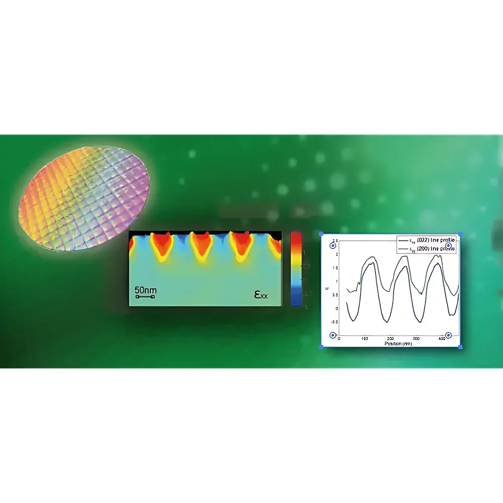
| Brand | NanoMEGAS |
|---|---|
| Origin | Belgium |
| Model | TopSPIN STRAIN |
| Application | Automated High-Resolution Strain Mapping in Scanning Transmission Electron Microscopy (STEM) using 4D Scanning Precession Electron Diffraction (4D-SPED) |
| Spatial Resolution | 2–3 nm (FEG-TEM) |
| Strain Sensitivity | < 2 × 10⁻⁴ |
| Typical Acquisition Time | 5–10 min (150 × 150 pixels) |
| Pixel Dwell Time | 10–40 ms |
| Strain Quantification Accuracy | ±0.02% (at 200 kV FEG-TEM) |
| Analysis Engine | AppFive proprietary algorithm |
| Output Modalities | Point, line, and 2D strain tensor maps (εₓₓ, ε_zz, ε_xz), orientation/phase/strain/STEM co-registration |
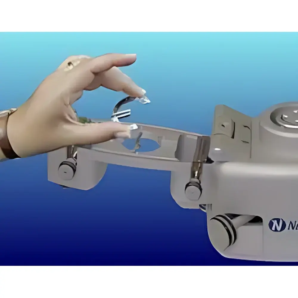
| Brand | Nanonics |
|---|---|
| Origin | Israel |
| Model | Academia |
| Instrument Type | Materials-Focused AFM |
| Primary Technique | Combined Scanning Probe Microscopy (SPM) with Integrated Near-Field Optical & Raman Capabilities |
| Scan Range | XY = 70 µm, Z = 5 µm (optional 10 µm scanner) |
| Positional Resolution | <1 nm (70 µm scanner), <0.1 nm (10 µm scanner) |
| Max Sample Size | 15 mm × 15 mm |
| Detection Method | Optical Beam Deflection |
| Operational Modes | Contact, Non-Contact, Tapping |
| Probe Compatibility | Nanonics glass probes, electro-thermal probes, NanoFountainPen™, and standard commercial SPM cantilevers |
| Software Platform | LabVIEW-based modular architecture with user-customizable modules |
| Compliance Ready | Designed for GLP/GMP-aligned workflows |
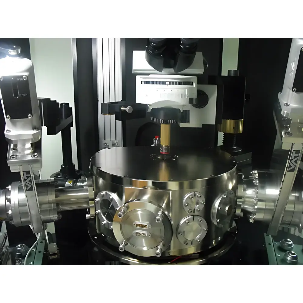
| Brand | Nanonics |
|---|---|
| Origin | Israel |
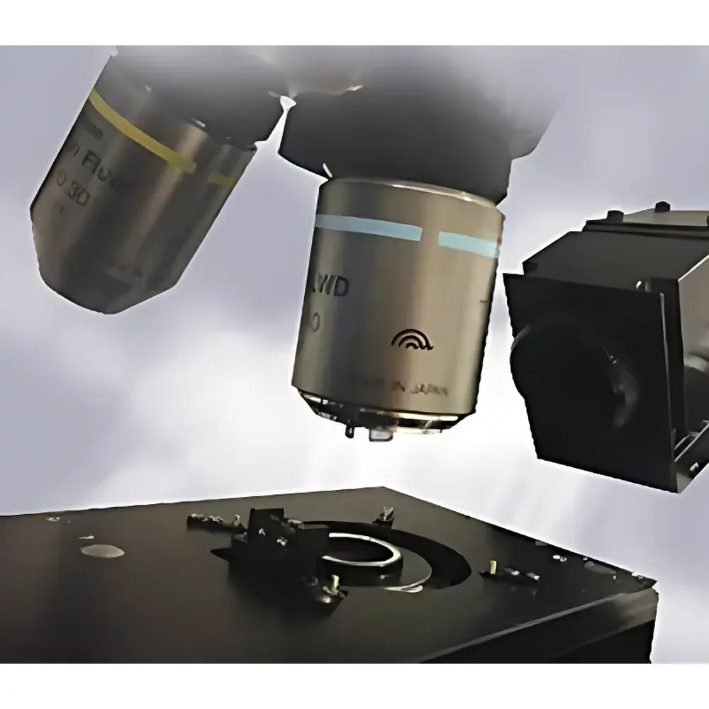
| Model | CryoView4000 |
| Z-positioning noise | <0.2 nm |
| Sample diameter | <100 mm |
| Sample thickness | <30 mm |
| Sample stage travel range | 80 µm × 80 µm × 70 µm |
| Brand | Nanonics |
|---|---|
| Origin | Israel |
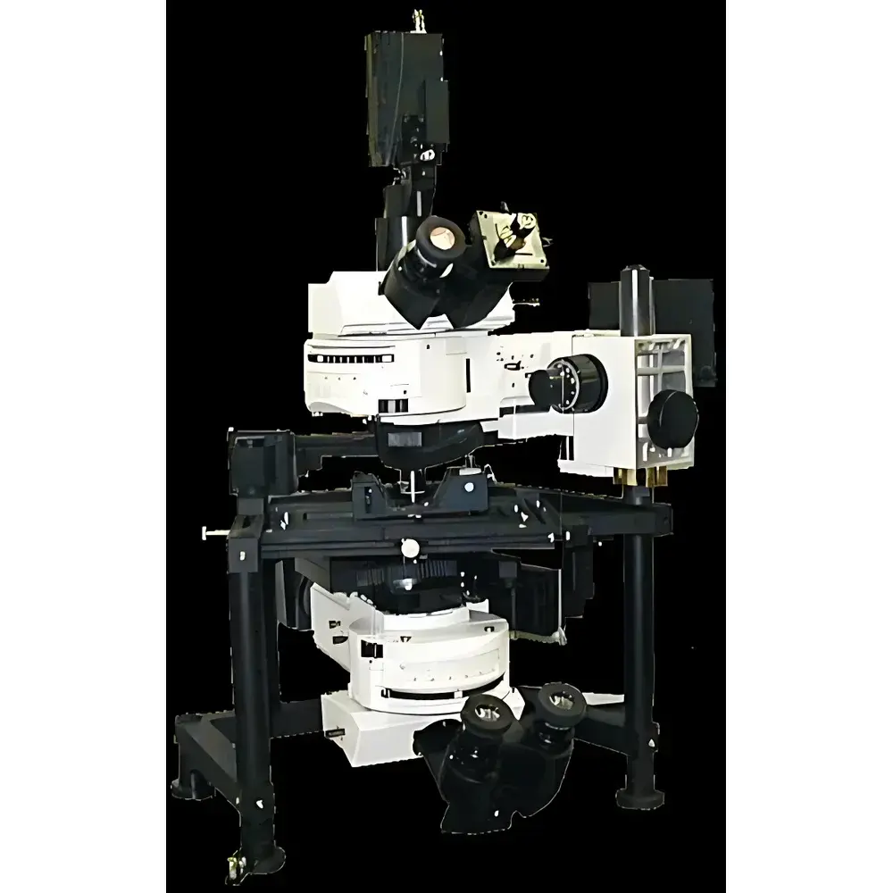
| Model | MultiView 2500 |
| Instrument Type | Hybrid SNOM/AFM System |
| Detection Noise (Positional) | 0.2 nm |
| Sample Size Capacity | 6 mm diameter |
| XYZ Scan Range per Stage | >80 µm |
| Dual-Stage Architecture | Probe Stage + Sample Stage |
| Feedback Mechanism | Tuning Fork (TF)-Based AFM |
| Optical Compatibility | Mid-IR to THz spectral range |
| Illumination/Collection Flexibility | Top-, Side-, and Bottom-Optical Access |
| Brand | Nanonics |
|---|---|
| Origin | Israel |
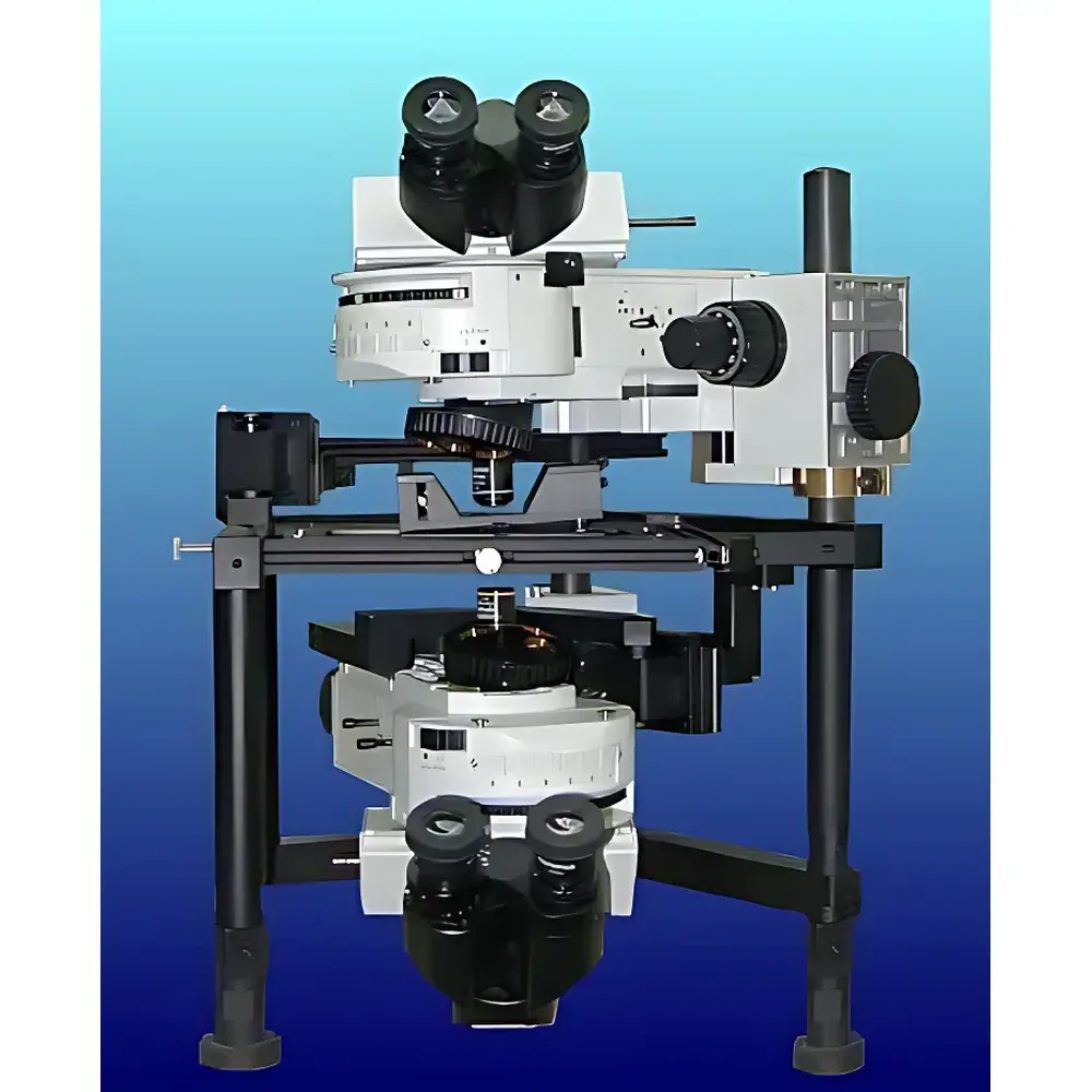
| Model | MultiView1000 |
| Instrument Type | Material-Focused AFM |
| Positional Noise | XY < 20 nm |
| Max Sample Diameter | < 100 mm |
| Max Sample Thickness | < 15 mm |
| Stage Travel Range | 85 µm × 85 µm |
| Brand | Nanonics |
|---|---|
| Origin | Israel |
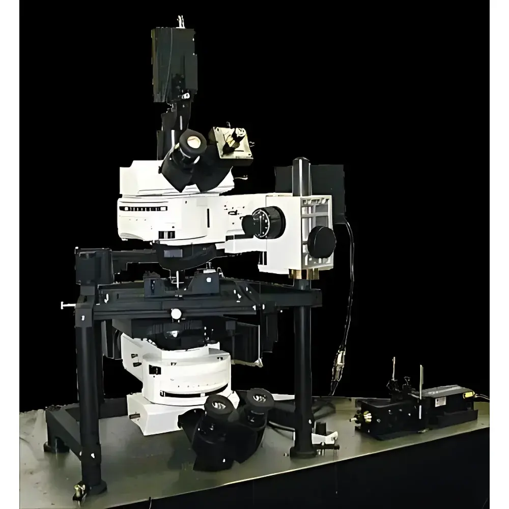
| Model | MultiView2000 |
| Instrument Type | Materials-Focused AFM/NSOM Hybrid System |
| Scan Mode | Tip Scanning |
| XY Resolution | <5 nm |
| Z Resolution | <1 nm |
| XY Scan Range | 70 µm (standard), optional 30 µm and 10 µm scanners |
| Z Scan Range | 70–120 µm |
| XY Step Size | <1 nm (70 µm scanner), <0.1 nm (10 µm scanner) |
| Scanner Thickness | 7 mm |
| Scanner Mass | 75 g |
| Max Sample Radius | 16 mm (customizable) |
| Probe Compatibility | Full commercial SPM probe interoperability including NSOM, conductive AFM, hollow probes, insulated nanowire sensors, dual-wire glass-insulated probes, low-k modulus probes, and deep-trench AFM probes |
| Operational Modes | NSOM reflection/transmission/collection/near-field fluorescence/PL |
| Controller | Nanonics Analog Controller with NT software (Windows 95/98/XP compatible) |
| Environmental Capabilities | Cryogenic operation down to 4 K (liquid helium), UHV compatibility, integrated gas/liquid delivery, in situ reaction chamber, co-located optical microscopy and micro-Raman coupling |
| Brand | Nanonics |
|---|---|
| Origin | Israel |
| Model | MultiView4000 |
| Instrument Type | Material-Focused AFM |
| Positioning Noise | XY < 20 nm |
| Sample Dimensions | Ø < 100 mm |
| Stage Travel Range | 170 µm × 170 µm |
| XY Resolution | < 5 nm |
| Z Resolution | < 1 nm |
| Scan Range (Combined Piezo + Sample Scanner) | up to 160 µm (XY) |
| Minimum Step Size | < 0.1 nm (10 µm scanner) |
| Scanner Thickness | 7 mm |
| Mass | 75 g |
| Probe Compatibility | Commercial SPM, NSOM, conductive, hollow, insulated glass nanowire, dual-wire, low-k AFM, deep-trench AFM probes |
| Operating Modes | NSOM reflection/transmission/collection/fluorescence/PL |
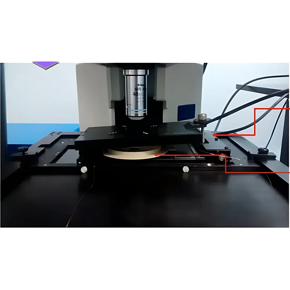
| Brand | Nanonics |
|---|---|
| Model | MV1000 / MV2000 / MV4000 |
| Instrument Type | AFM-Integrated Scanning Electrochemical Microscope |
| Z-Positioning Noise | 0.2 nm |
| Sample Diameter | < 6 mm |
| XYZ Scan Range | 80 µm × 80 µm × 80 µm |
| Probe | Hollow glass nanopipette with Pt nanowire electrode (50–100 nm tip diameter) |
| Electrochemical Control | Bipotentiostat (±10 V, ±0.25 A), current sensitivity: 10⁻¹²–0.1 A/V |
| Compatible Electrodes | Up to four side-mounted or back-contacted reference/counter electrodes (e.g., Ag/AgCl) |
| Liquid Cell Material | PEEK |
| Optical Access | Fully open top and bottom optical pathways |
| Environmental Options | Optional inert-gas chamber (N₂/Ar) |
| Software Compliance | Supports audit trail, user access control, and data integrity per FDA 21 CFR Part 11 requirements |