
Scanning Electron Microscope
Filter
Showing 31–60 of 153 results
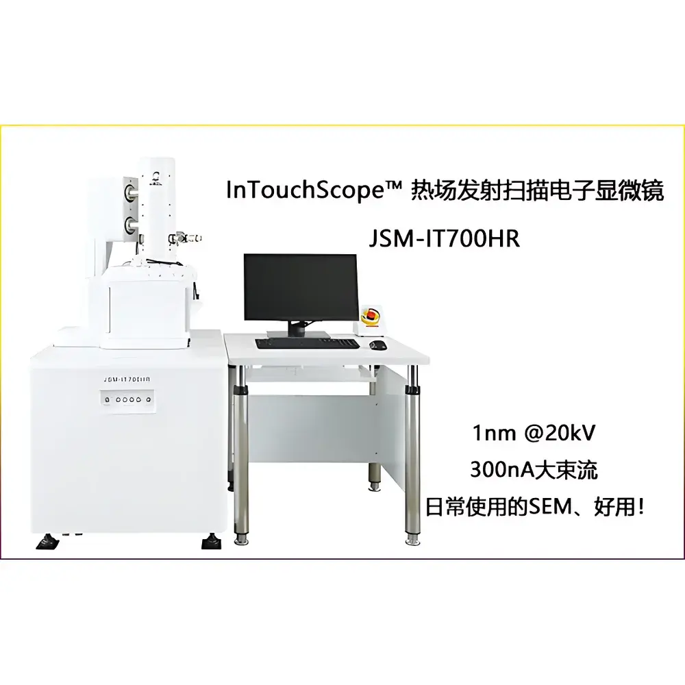
| Brand | JEOL |
|---|---|
| Origin | Japan |
| Model | JSM-IT710HR |
| Instrument Type | Benchtop SEM |
| Electron Source | Thermal Field Emission Gun (TFEG) |
| Secondary Electron Resolution | 1 nm @ 30 kV |
| Backscattered Electron Resolution | 2 nm @ 30 kV |
| Accelerating Voltage | 0.1–30 kV |
| Maximum Magnification | 1,000,000× |
| Probe Current | Up to 300 nA |
| Sample Chamber | Large-volume, front-loading with wide-access door |
| Operating Modes | High Vacuum / Low Vacuum (LV/LA variants available) |
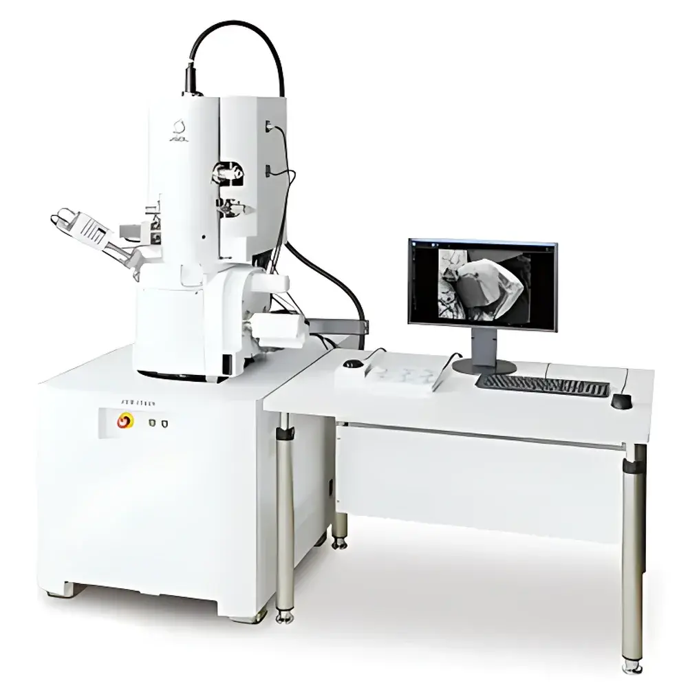
| Brand | JEOL |
|---|---|
| Origin | Japan |
| Model | JSM-IT800 |
| Instrument Type | Floor-Standing SEM |
| Electron Source | Thermal Field-Emission Gun (TFEG) |
| Secondary Electron Resolution | 0.6 nm @ 15 kV, 0.7 nm @ 1 kV |
| Backscattered Electron Resolution | 1.5 nm |
| Accelerating Voltage Range | 0.01–30 kV |
| Maximum Magnification | 2,000,000× (real) |
| Specimen Diameter Capacity | 150 mm |
| Stage Type | 5-Axis Motorized Precision Stage |
| Detector Configuration | In-lens SE detector, upper-stage BSE detector, optional EDS/WDS integration |
| Beam Current | ≥300 nA @ 15 kV |
| Objective Lens Design | Super Hybrid Objective Lens (Magnetic-Field-Free) |
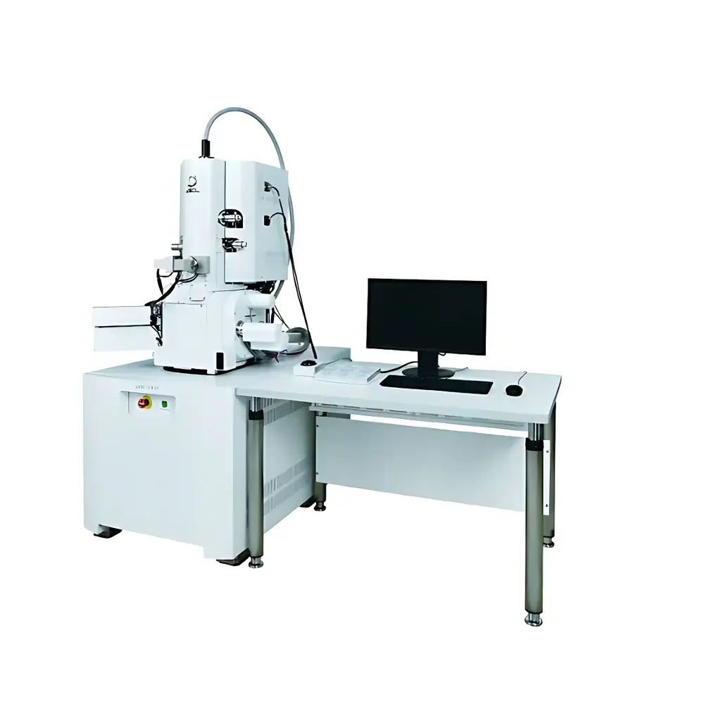
| Brand | JEOL |
|---|---|
| Origin | Japan |
| Model | JSM-IT810 |
| Instrument Type | Floor-standing SEM |
| Electron Gun | Thermal Field Emission (TFE) |
| Secondary Electron (SE) Resolution | 0.5 nm at 15 kV |
| Backscattered Electron (BSE) Resolution | 1.5 nm at 15 kV |
| Accelerating Voltage Range | 0.01–30 kV |
| Magnification Range | ×27 to ×5,480,000 (at 1280 × 960 pixels) |
| Beam Current | Up to 500 nA |
| Detector Configuration | Standard In-lens SE, Through-the-lens BSE, and Optional EDS/EBSD Integration |
| Sample Chamber | Expandable with Multiple Ports for In-situ & Analytical Add-ons |
| Stage | Motorized, High-Precision 5-Axis Tilt/Rotation/Translation Stage |
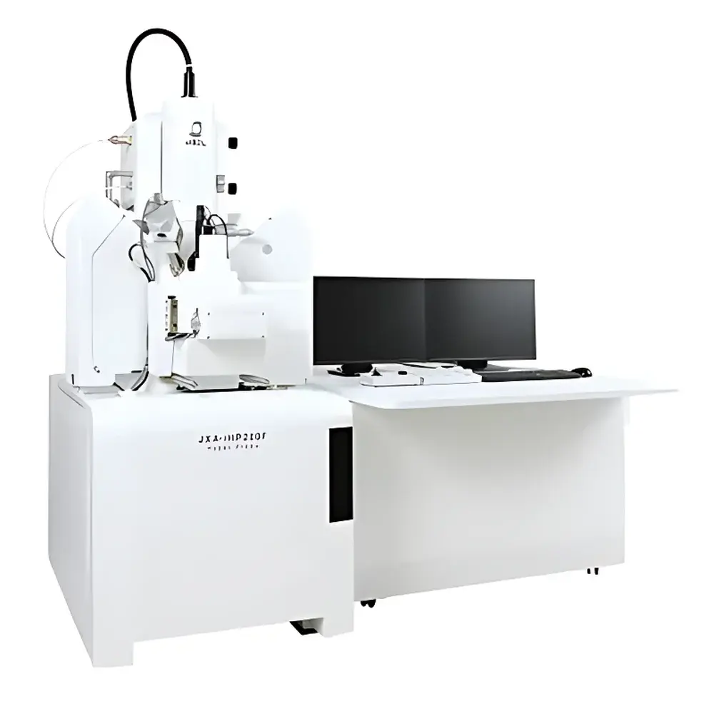
| Brand | JEOL |
|---|---|
| Origin | Japan |
| Model | JXA-iHP200F |
| Instrument Type | Floor-standing, High-Performance EPMA |
| Electron Source | Thermal Field-Emission Gun (TFEG) |
| Secondary Electron Resolution | 2.5 nm at 15 kV |
| Magnification Range | 40× to 300,000× |
| Accelerating Voltage | 1–30 kV |
| Backscattered Electron Imaging | High-Contrast Mode |
| Maximum Sample Dimensions | 100 mm × 100 mm × 50 mm (H) |
| Motorized Stage | 5-Axis Precision Drive |
| Standard Detectors | Solid-State Backscatter Detector, Wavelength-Dispersive Spectrometer (WDS), Energy-Dispersive Spectrometer (EDS) |
| Vacuum System | Ultra-High Vacuum (UHV) Compatible |
| Interface Expansion | Multiple Dedicated Ports for Optional Analyzers (e.g., EBSD, CL, STEM-in-SEM) |
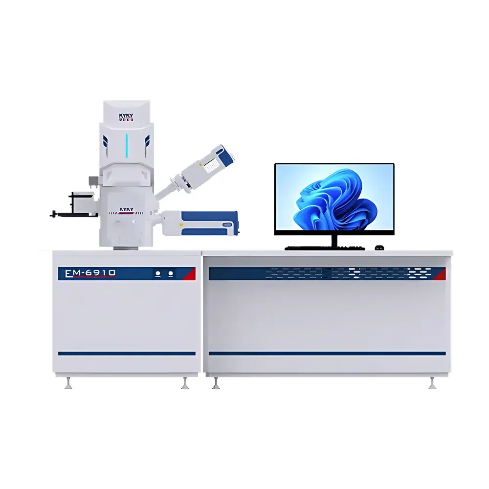
| Brand | KYKY |
|---|---|
| Origin | Beijing, China |
| Manufacturer Type | Direct Manufacturer |
| Instrument Class | Floor-Standing Conventional SEM |
| Electron Source | Tungsten Filament |
| SEM Category | Entry-Level Tungsten-Filament SEM |
| Secondary Electron (SE) Resolution | 3 nm @ 30 kV, 8 nm @ 3 kV |
| Accelerating Voltage Range | 0.2–30 kV |
| Backscattered Electron (BSE) Resolution | 4 nm @ 30 kV |
| Sample Chamber | Optional Large-Capacity Chamber |
| Vacuum Mode | Compatible with Low-Vacuum Module |
| Load Lock System | Max. Sample Diameter ≤75 mm, Height ≤15 mm |
| Navigation Camera | Integrated Wide-Field CCD Navigation Camera |
| Imaging Modes | Simultaneous SE/BSE Dual-Channel Imaging |
| Image Stitching | Automated Full-Field Matrix Acquisition & Real-Time High-Throughput Mosaic Reconstruction |
| Particle Analysis | AI-Driven Morphometric Quantification (size, aspect ratio, circularity, convexity, Feret diameter, etc.) with Auto-Scale Calibration |
| Metrology Tools | Distance, Angle, Line (horizontal/vertical), Circle Diameter, and Profile Analysis |
| Electron Beam Lithography (EBL) Capability | Integrated Vector-Scan EBL Subsystem Supporting Pattern Definition, Dose Control, and Concurrent SEM Observation |
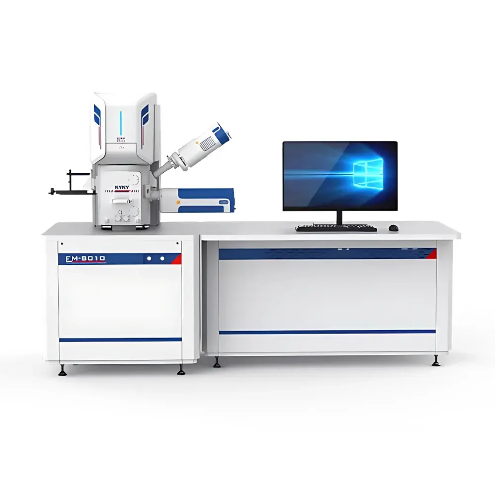
| Brand | KYKY |
|---|---|
| Origin | Beijing, China |
| Manufacturer Type | Direct Manufacturer |
| Instrument Type | Floor-standing SEM |
| Electron Gun Type | Schottky Thermal Field Emission |
| SEM Class | Entry-level Field Emission SEM |
| Secondary Electron Resolution | 1.5 nm @ 15 kV |
| Accelerating Voltage Range | 0.2–30 kV |
| Backscattered Electron Resolution | 3 nm @ 30 kV |
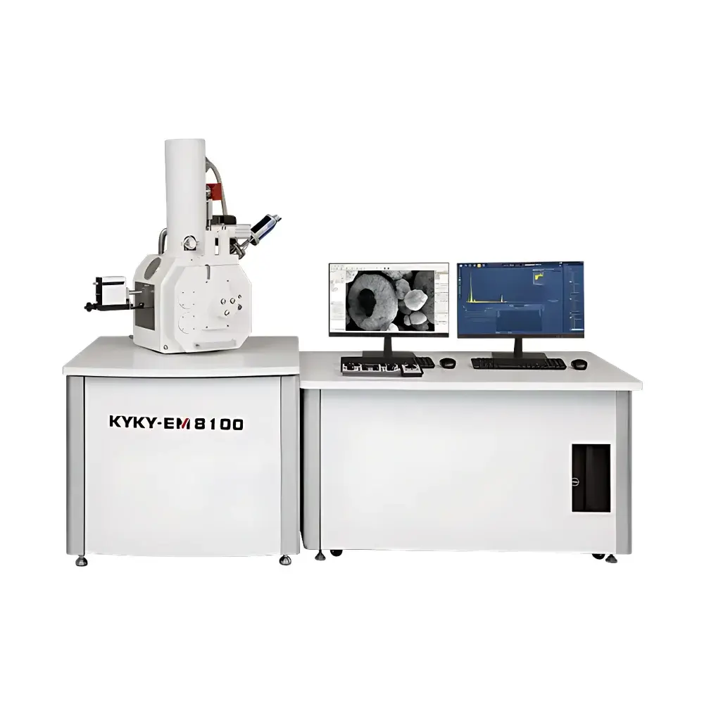
| Brand | KYKY |
|---|---|
| Origin | Beijing, China |
| Manufacturer Type | Original Equipment Manufacturer (OEM) |
| Instrument Type | Floor-Model SEM |
| Electron Gun | Thermal Field-Emission (TFE) |
| SEM Class | High-Resolution Field-Emission SEM |
| Secondary Electron (SE) Resolution | 0.9 nm @ 30 kV |
| Magnification Range | 1×–3,000,000× (optical: 1×–100×) |
| Accelerating Voltage | 0.2–30 kV |
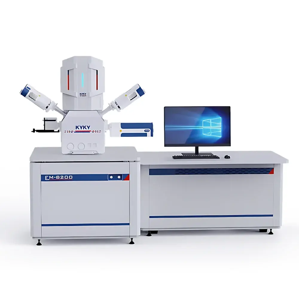
| Brand | KYKY |
|---|---|
| Origin | Beijing, China |
| Manufacturer Type | Direct Manufacturer |
| Instrument Type | Floor-Standing SEM |
| Electron Gun | Thermal Field Emission |
| SEM Class | Ultra-High-Resolution Field Emission |
| Secondary Electron Resolution | 0.8 nm @ 15 kV, 1.5 nm @ 1 kV |
| Magnification Range | 1×–3,000,000× (electronic), 1×–100× (optical) |
| Accelerating Voltage | 0.2–30 kV |
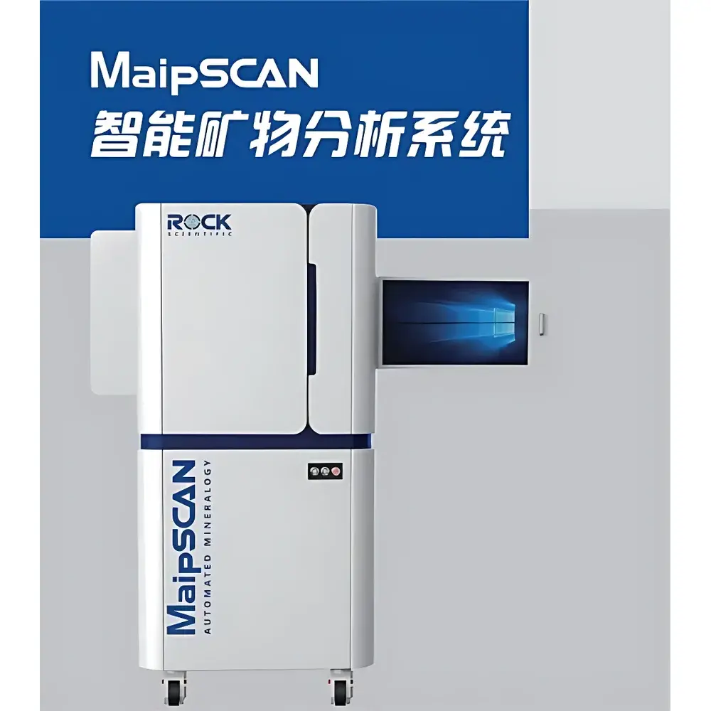
| Brand | ROCK |
|---|---|
| Origin | Hong Kong, China |
| Model | MaipSCAN |
| Instrument Type | Floor-standing SEM |
| Electron Source | Tungsten Filament |
| Secondary Electron Resolution | 3.0 nm @ 30 kV (SE and W) |
| Magnification Range | 7× – 1,000,000× |
| Accelerating Voltage | 0.2 – 30 kV |
| Backscattered Electron Resolution | 4.0 nm @ 30 kV (VP mode with BSD) |
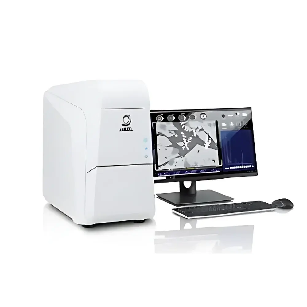
| Brand | Narishige |
|---|---|
| Origin | Japan |
| Model | JCM-7000 |
| Instrument Type | Desktop SEM |
| Magnification Range | 10×–100,000× (print output: 128 mm × 96 mm) |
| 24×–202,168× (on-screen display | 280 mm × 210 mm) |
| Accelerating Voltage | 5 kV, 10 kV, or 15 kV (software-selectable constant-voltage mode) |
| BSE Image Resolution | Not specified (system optimized for compositional and topographic contrast) |
| Specimen Dimensions | Ø80 mm × 50 mm (without stage夹具) |
| Detector Types | Everhart-Thornley secondary electron detector |
| Stage Motion | Motorized X/Y = ±40 mm each |
| Tilt | −15° to +45° |
| Rotation | 360° continuous |
| Vacuum Modes | High Vacuum (HV) and Low Vacuum (LV) |
| Operating System | Windows 10 |
| Data Formats | TIFF, BMP, JPEG, PNG (still) |
| Electron Source | Tungsten filament with integrated Wehnelt cap |
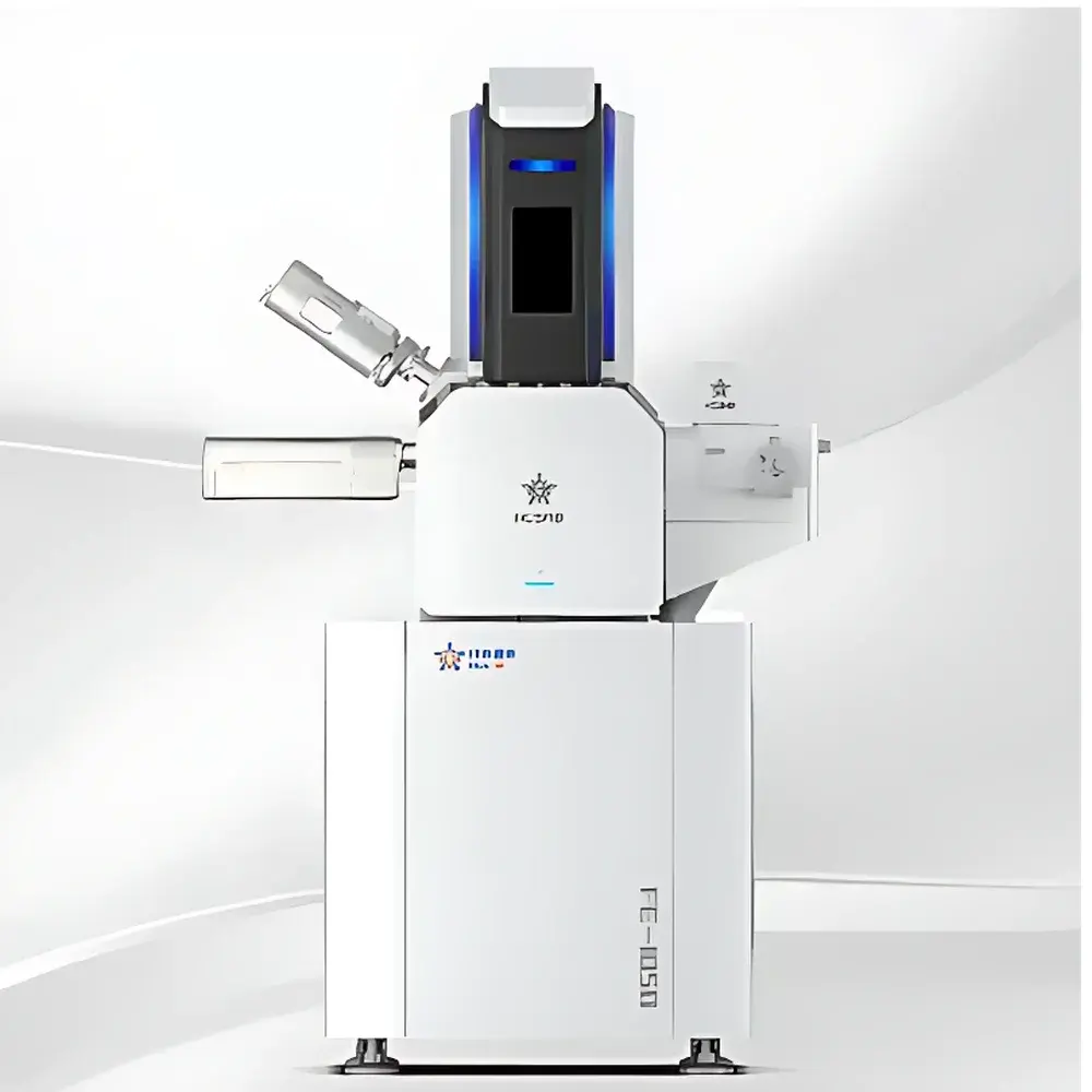
| Brand | NCS |
|---|---|
| Origin | Beijing, China |
| Manufacturer Type | Direct Manufacturer |
| Product Category | Domestic |
| Model | FE-1050 Series |
| Instrument Form Factor | Floor-Standing |
| Electron Gun Type | Thermal Field Emission |
| Secondary Electron (SE) Resolution | 1.5 nm @ 1 kV, 0.9 nm @ 15 kV |
| Magnification Range | 10× to 1,000,000× |
| Accelerating Voltage | 0.02–30 kV |
| Backscattered Electron (BSE) Resolution | 2.5 nm @ 1 kV, 1.5 nm @ 15 kV |
| Sample Chamber Port Count | 27 |
| Stage Motion | 5-Axis Motorized (X = 140 mm, Y = 140 mm, Z = 60 mm, Rotation = 360°, Tilt = −10° to +80°) |
| Standard Detectors | In-Column SE Detector, Everhart-Thornley SE Detector, Optional Insertable BSE Detector, Optional STEM Detector, Triple-Channel IR CCD Chamber Monitoring System |
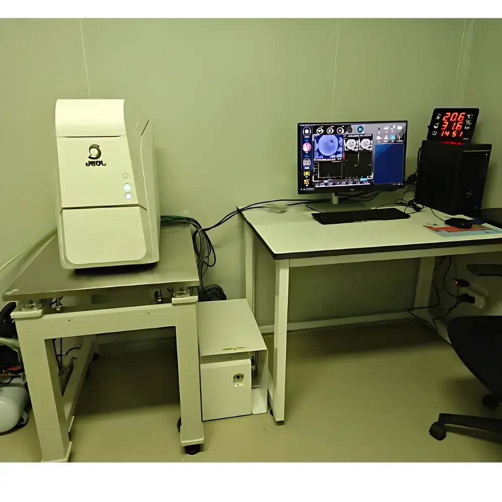
| Brand | NIKON |
|---|---|
| Origin | Japan |
| Manufacturer Type | Authorized Distributor |
| Origin Category | Imported |
| Model | JCM-7000 |
| Instrument Type | Desktop SEM |
| Electron Gun | Tungsten Filament |
| SEM Class | Entry-Level Tungsten-Filament SEM |
| Secondary Electron Image Resolution | 20 nm |
| Magnification Range | 10×–60,000× |
| Accelerating Voltages | 5 kV, 10 kV, 15 kV |
| Backscattered Electron Image Resolution | 20 nm |
| Vacuum Modes | High Vacuum & Low Vacuum |
| Sample Chamber Capacity | Ø ≥80 mm × H ≥50 mm |
| Motorized Stage Travel | X ≥40 mm, Y ≥40 mm |
| Detector Configuration | Secondary Electron Detector (SED) + Backscattered Electron Detector (BSED) |
| Imaging Modes | SE, BSE (compositional & topographic), Real-Time 3D Reconstruction |
| Dual-Channel Simultaneous Display | Yes |
| Image Storage Resolutions | 1280×960, 2560×1920, 5120×3840 pixels |
| Power Supply | AC 100–240 V, 50/60 Hz, ≤700 VA |
| Operating Temperature | 15–30 °C |
| Relative Humidity | 30–60 % RH (non-condensing) |
| Ground Resistance | <100 Ω |
| Brand | Opton |
|---|---|
| Origin | Germany |
| Distributor Type | Authorized Distributor |
| Import Status | Imported |
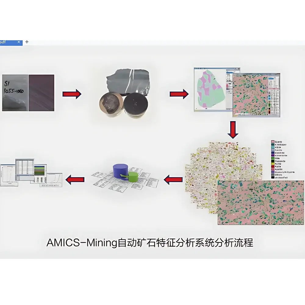
| Model | AMICS |
| Electron Gun | Tungsten Filament |
| Secondary Electron Resolution | 3.0 nm @ 30 kV (SE, W) |
| Magnification Range | 5× – 1,000,000× |
| Accelerating Voltage | 0.2–30 kV |
| Backscattered Electron Resolution | 4.0 nm @ 30 kV (VP with BSD) |
| Minimum Detectable Mineral Grain Size | 1 µm |
| Typical Measurement Time (30 mm diameter sample) | 15 min |
| Mineral Database | >2,000 reference minerals |
| Stage | High-precision 5-axis motorized 9-pin stage |
| EDS Detector Compatibility | Silicon Drift Detector (SDD), liquid-nitrogen-free cryogenic cooling, ultra-fast pulse processing (e.g., Bruker QUANTAX) |

| Brand | Oxford Instruments |
|---|---|
| Origin | United Kingdom |
| Manufacturer Type | Authorized Distributor |
| Origin Category | Imported |
| Model | AZtecFeature |
| Instrument Type | Benchtop SEM-EDS System |
| Electron Source | Tungsten Filament |
| Secondary Electron Resolution | 1.0 nm @ 15 kV, WD = 4 mm |
| Magnification Range | 20–2,000× (low mag) |
| Accelerating Voltage | 1–30 kV |
| Backscattered Electron Resolution | 4 nm @ 30 kV (low-vacuum mode) |
| Detector Configuration | Up to four Ultim Max SDDs supported |
| Real-time Particle Counting Capacity | Up to 200,000 particles per sample |
| Data Acquisition & Quantification Engine | Tru-Q® automated elemental identification and quantification |
| Peak Deconvolution | Advanced sum-peak correction for high-count-rate accuracy |
| Software Architecture | Native 64-bit multithreaded processing |
| Compliance | ASTM E1588–10e1 (GSR), ISO 16232 (cleanliness), VDA 19.1, USP <788>, GLP/GMP-aligned audit trail support |
| Brand | Phenom |
|---|---|
| Origin | Netherlands |
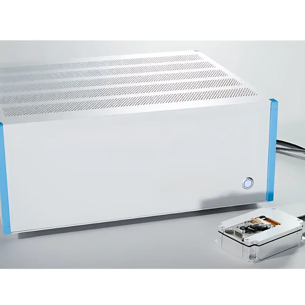
| Model | Phenom AFM-SEM |
| Instrument Type | Benchtop SEM-AFM Hybrid System |
| Electron Source | Cerium Hexaboride (CeB₆) |
| Maximum Sample Dimensions | 21 mm × 11 mm × 8 mm |
| Scan Range (Open-Loop) | 100 µm × 100 µm × 20 µm |
| Scan Range (Closed-Loop) | 80 µm × 80 µm × 16 µm |
| Spatial Resolution | 0.2 nm (lateral) × 0.04 nm (vertical) |
| Sample Mass Limit | 100 g |
| Imaging Modes | Topography & Roughness, Conductive AFM (CAFM), Kelvin Probe Force Microscopy (KPFM), Magnetic Force Microscopy (MFM), Piezoresponse Force Microscopy (PFM), Electrostatic Force Microscopy (EFM), Force–Distance (F–z) Curves, Current–Voltage (I–V) Spectroscopy |
| Brand | Phenom |
|---|---|
| Origin | Netherlands |
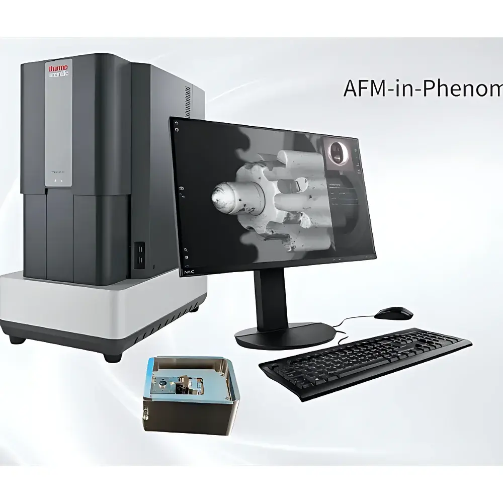
| Model | AFM-in-Phenom XL |
| Instrument Type | Benchtop SEM-AFM Hybrid System |
| Electron Source | Cerium Hexaboride (CeB₆) |
| Maximum Sample Dimensions | 21 mm × 11 mm × 8 mm |
| Sample Weight Limit | 100 g |
| Open-Loop Scan Range | 100 µm × 100 µm × 20 µm |
| Closed-Loop Scan Range | 80 µm × 80 µm × 16 µm |
| Spatial Resolution (XY/Z) | 0.2 nm × 0.2 nm / 0.04 nm |
| Compatible Modes | Topography, Roughness, CAFM, KPFM, FMM, PFM, EFM, Force-Distance (F-z), Current-Voltage (I-V) |
| Brand | Phenom |
|---|---|
| Origin | Netherlands |
| Model | Phenom Ar-C |
| Instrument Type | Benchtop SEM |
| Electron Source | Cerium Hexaboride (CeB6) |
| Secondary Electron Resolution | 8 nm |
| Maximum Magnification | 200,000× |
| Accelerating Voltage Range | 4.8–20.5 kV |
| Backscattered Electron Resolution | 8 nm |
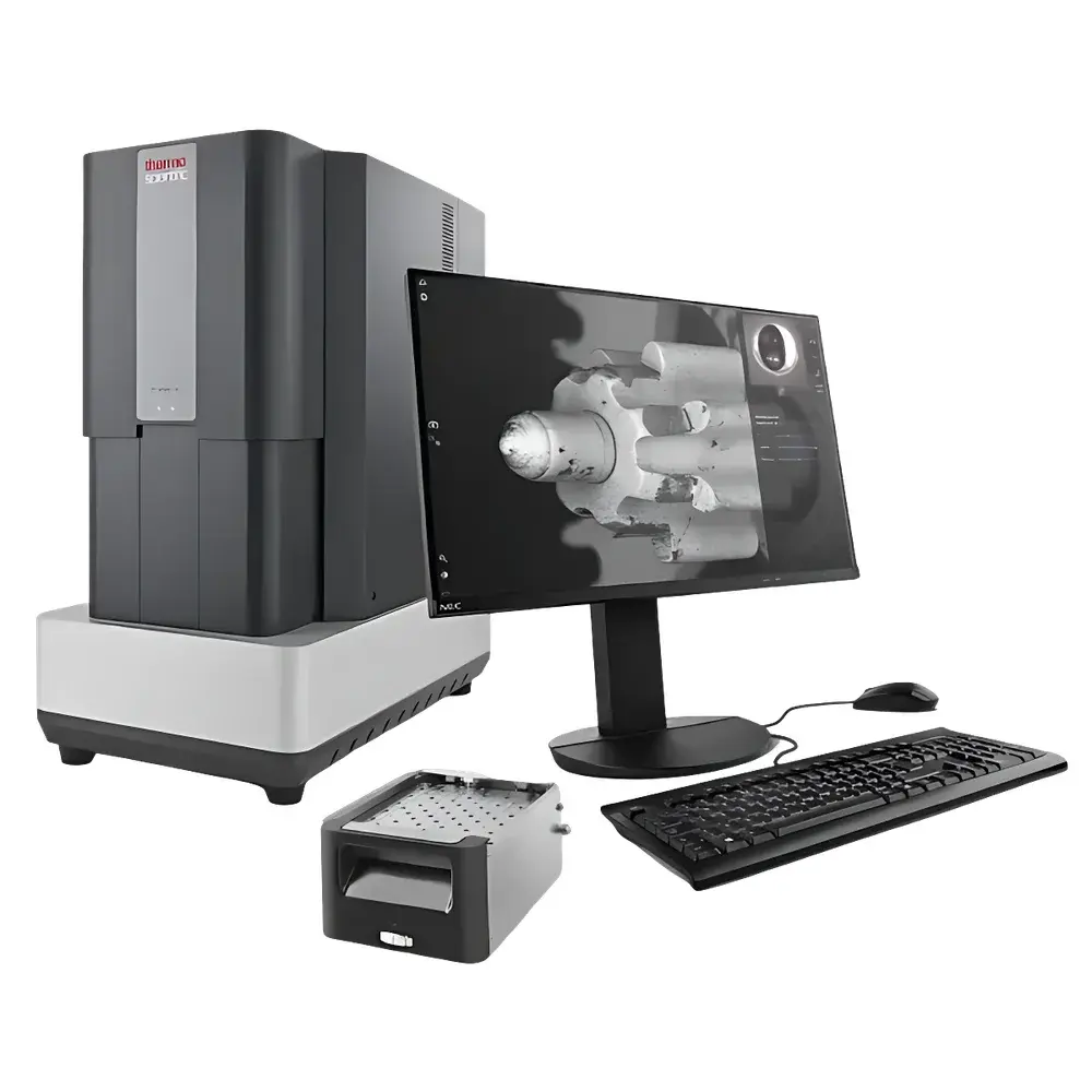
| Brand | Phenom |
|---|---|
| Origin | Netherlands (Manufactured in Guangzhou, China) |
| Type | Benchtop SEM |
| Electron Source | Cerium Hexaboride (CeB6) |
| SEM Class | Entry-level Field Emission / Tungsten-Filament Hybrid Architecture |
| Secondary Electron Resolution | 8 nm @ 20 kV |
| Backscattered Electron Resolution | 8 nm @ 20 kV |
| Magnification Range | 20× – 200,000× |
| Accelerating Voltage | 4.8 – 20.5 kV |
| Vacuum Pumping Time | ≤15 s |
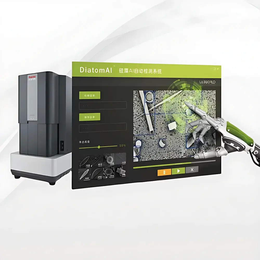
| Brand | Phenom |
|---|---|
| Origin | Netherlands |
| Manufacturer | Phenom-World B.V. |
| Type | Desktop SEM |
| Model | DiatomScopeTM |
| Electron Source | CeB₆ (Cerium Hexaboride) |
| Secondary Electron Resolution | 8 nm |
| Backscattered Electron Resolution | 8 nm |
| Magnification Range | up to 200,000× |
| Accelerating Voltage | 4.8–20.5 kV |
| Sample Stage | Motorized XY-stage with automated tilt & rotation |
| Imaging Modes | SE, BSE, EDS-ready |
| Software Platform | Phenom Desktop Software v5.x with Diatom Analysis Module |
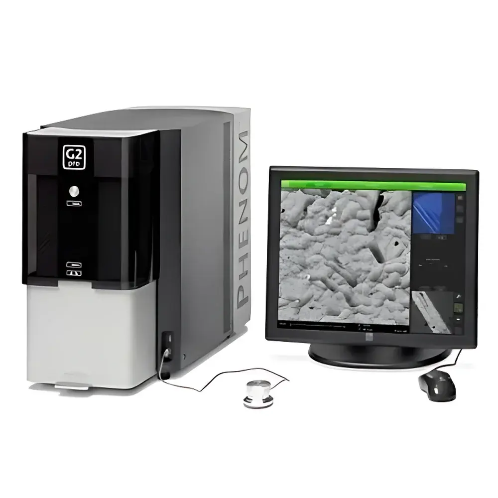
| Brand | SHNTI |
|---|---|
| Origin | Netherlands |
| Manufacturer Type | Authorized Distributor |
| Origin Category | Imported |
| Model | Phenom G2 |
| Price Range | USD 70,000–140,000 |
| Instrument Type | Benchtop SEM |
| Electron Source | Lanthanum Hexaboride (LaB₆) |
| Secondary Electron Image Resolution | ≤5.0 nm at 10 kV |
| Magnification Range | 10×–130,000× |
| Accelerating Voltage | 5–15 kV (adjustable in 1 kV steps) |
| Backscattered Electron Image Resolution | ≤7.0 nm at 10 kV |
| Maximum Sample Dimensions | 100 mm diameter × 50 mm height |
| Expandable Chamber Interface Ports | 1 (for optional EDS or cathodoluminescence modules) |
| Stage Type | Motorized XY-stage with tilt (±90°), rotation (360°), and Z-height adjustment |
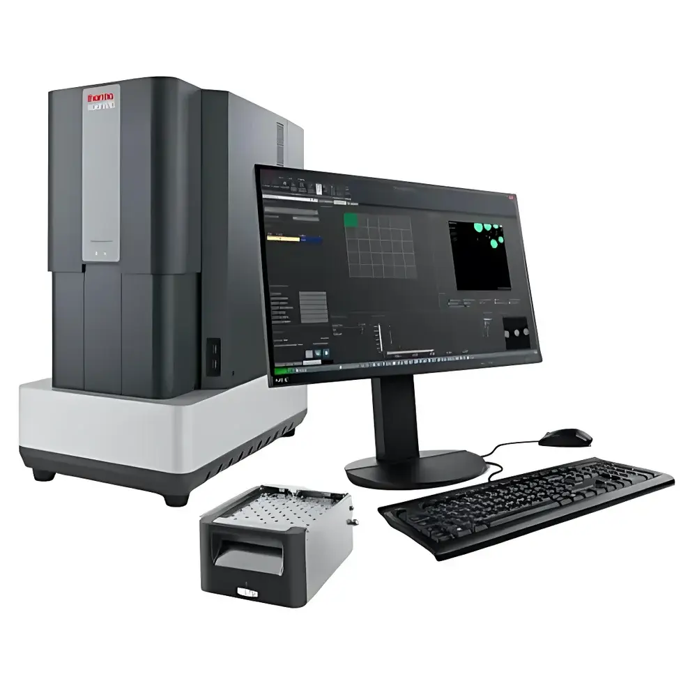
| Brand | Phenom |
|---|---|
| Origin | Netherlands |
| Manufacturer Type | Manufacturer |
| Origin Category | Imported |
| Model | Phenom GSR |
| Instrument Type | Benchtop SEM |
| Electron Source | Cerium Hexaboride (CeB6) |
| Secondary Electron Resolution | 8 nm |
| Maximum Magnification | 200,000× |
| Accelerating Voltage Range | 4.8–20.5 kV |
| Backscattered Electron Resolution | 8 nm |
| Maximum Sample Dimensions | 100 mm × 100 mm × 65 mm |
| Sample Capacity | Up to 36 × 12.7 mm (0.5″) stubs |
| Optical Navigation Camera | Integrated color CCD |
| Lamp Lifetime | ≥1500 h |
| Load Time | <60 s |
| Vacuum Modes | High Vacuum / Low-Voltage Mode (reduced charging) |
| Detectors | Integrated BSED, Optional SE Detector |
| EDS Integration | Fully embedded energy-dispersive X-ray spectrometer |
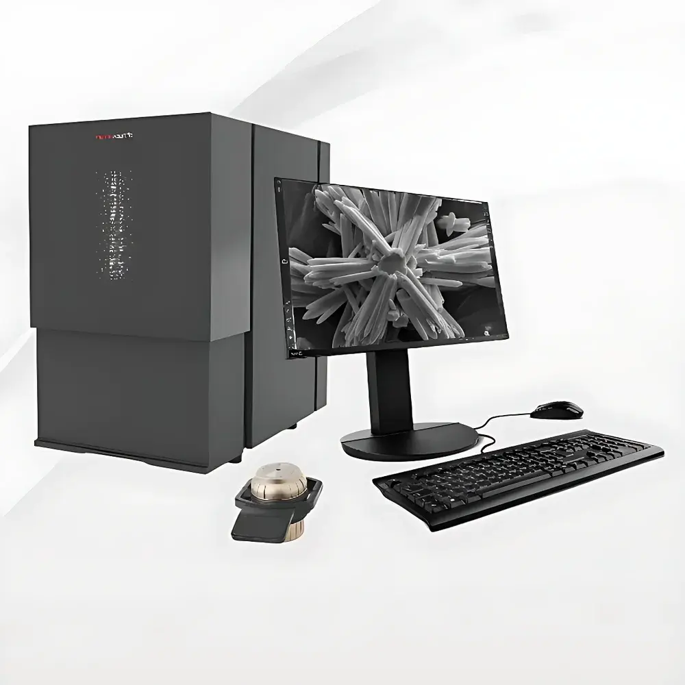
| Brand | Phenom |
|---|---|
| Origin | Netherlands |
| Manufacturer | Thermo Fisher Scientific (Phenom brand) |
| Type | Desktop SEM |
| Electron Source | Schottky Field-Emission |
| Imaging Modes | Secondary Electron (SE) & Backscattered Electron (BSE) |
| SE Resolution | ≤2.5 nm @ 15 kV |
| BSE Resolution | ≤2.5 nm @ 15 kV |
| Max Magnification | 1,000,000× |
| Vacuum Cycle Time | <15 s |
| Sample Compatibility | Conductive & Non-conductive (uncoated), Magnetic |
| Navigation | Integrated Color Optical Microscope with Panoramic View |
| Stage | Motorized XYZ Stage with Auto-Align |
| Vibration Isolation | Built-in 27-Element Passive Damping System |
| Maintenance | Field-Emission Source Lifetime >2,000 h |
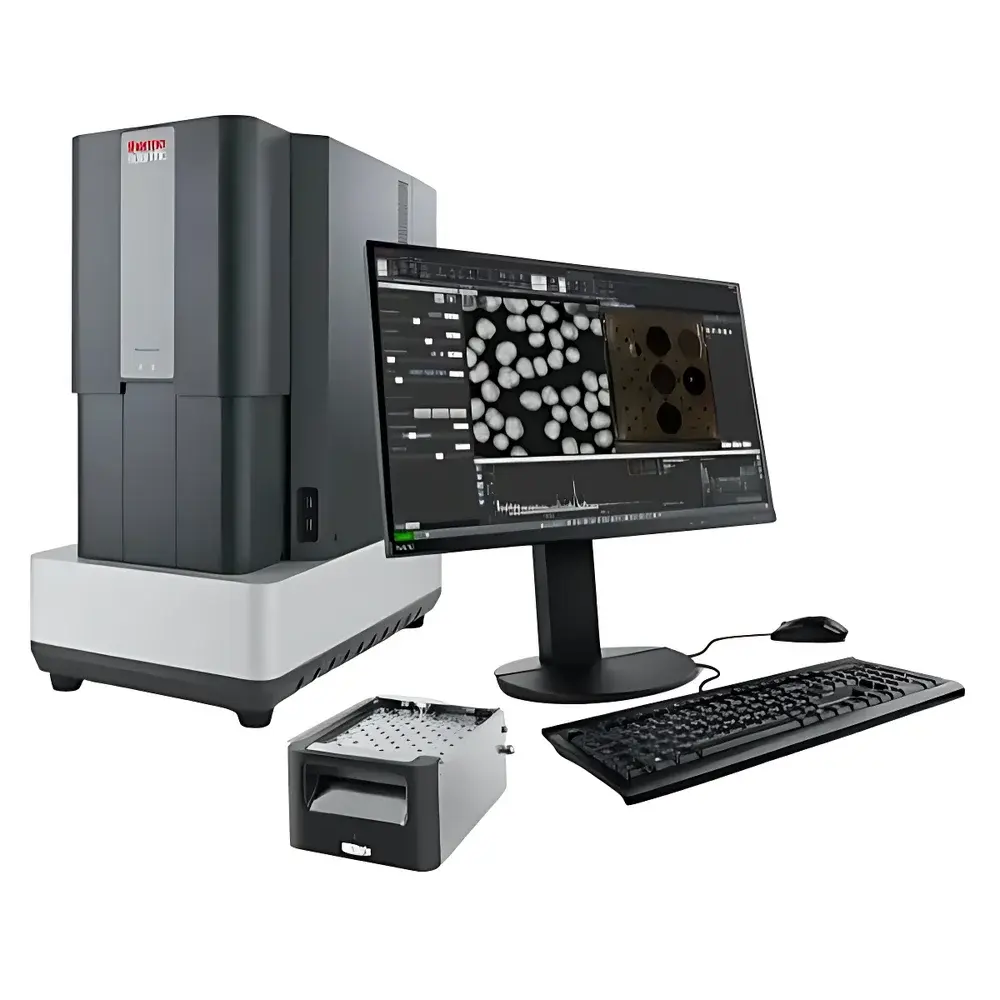
| Brand | Phenom |
|---|---|
| Origin | Netherlands |
| Manufacturer | Phenom-World B.V. |
| Product Type | Desktop Scanning Electron Microscope (SEM) |
| Model | ParticleX Li-Battery |
| Electron Source | CeB6 (Cerium Hexaboride) |
| Secondary Electron Resolution | 8 nm |
| Maximum Magnification | 200,000× |
| Acceleration Voltage Range | Standard Modes: 2 kV, 5 kV, 10 kV, 15 kV, 20 kV |
| Advanced Mode | Continuously Adjustable from 4.8 kV to 20.5 kV |
| Backscattered Electron Resolution | 8 nm |
| Standard Detectors | Backscattered Electron Detector (BSE), Energy Dispersive X-ray Spectrometer (EDS) |
| Optional Detector | Secondary Electron Detector (SED) |
| Sample Stage | Motorized 100 × 100 mm XY Stage |
| Vacuum System | Triple-chamber Separated Design, Pump-down Time < 60 s |
| Filament Lifetime | > 3000 h (CeB6, Warranty Guaranteed) |
| Compliance | ASTM E1508, ISO 16700, USP <1086>, GLP/GMP-Aligned Data Integrity Framework |
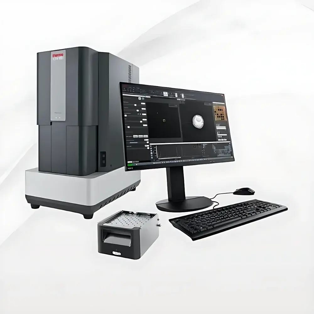
| Brand | Phenom |
|---|---|
| Origin | Netherlands |
| Manufacturer | Phenom-World B.V. |
| Product Type | Desktop Scanning Electron Microscope (SEM) |
| Model | ParticleX |
| Electron Source | Cerium Hexaboride (CeB6) |
| Maximum Magnification | 200,000× |
| Accelerating Voltage | Standard Modes: 2 kV, 5 kV, 10 kV, 15 kV, 20 kV |
| Advanced Mode | Continuously Adjustable from 4.8 kV to 20.5 kV |
| Backscattered Electron (BSE) Image Resolution | ≤ 8 nm |
| Standard Detectors | High-Sensitivity Quad-BSE Detector, Energy-Dispersive X-ray Spectrometer (EDS) |
| Optional Detector | Secondary Electron (SE) Detector |
| Vacuum Pumping Time | < 30 s |
| Lamp Lifetime | ~3,000 h |
| Operating Environment | Standard Lab or Office (Active Vibration Isolation Integrated) |
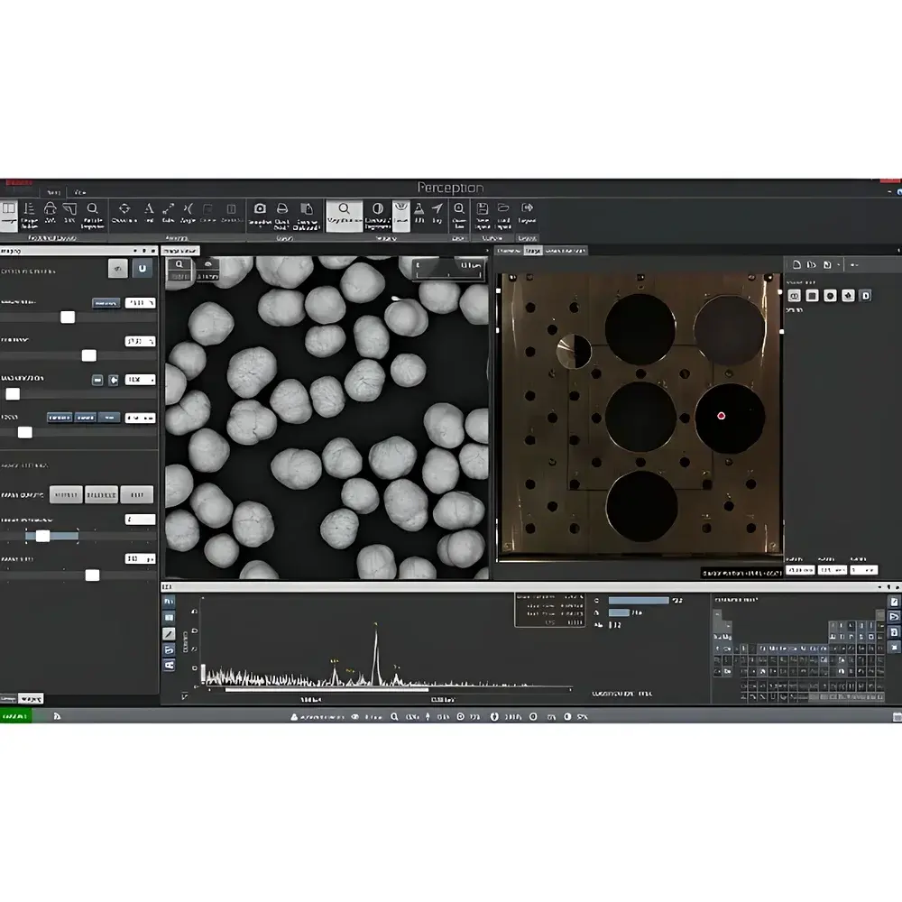
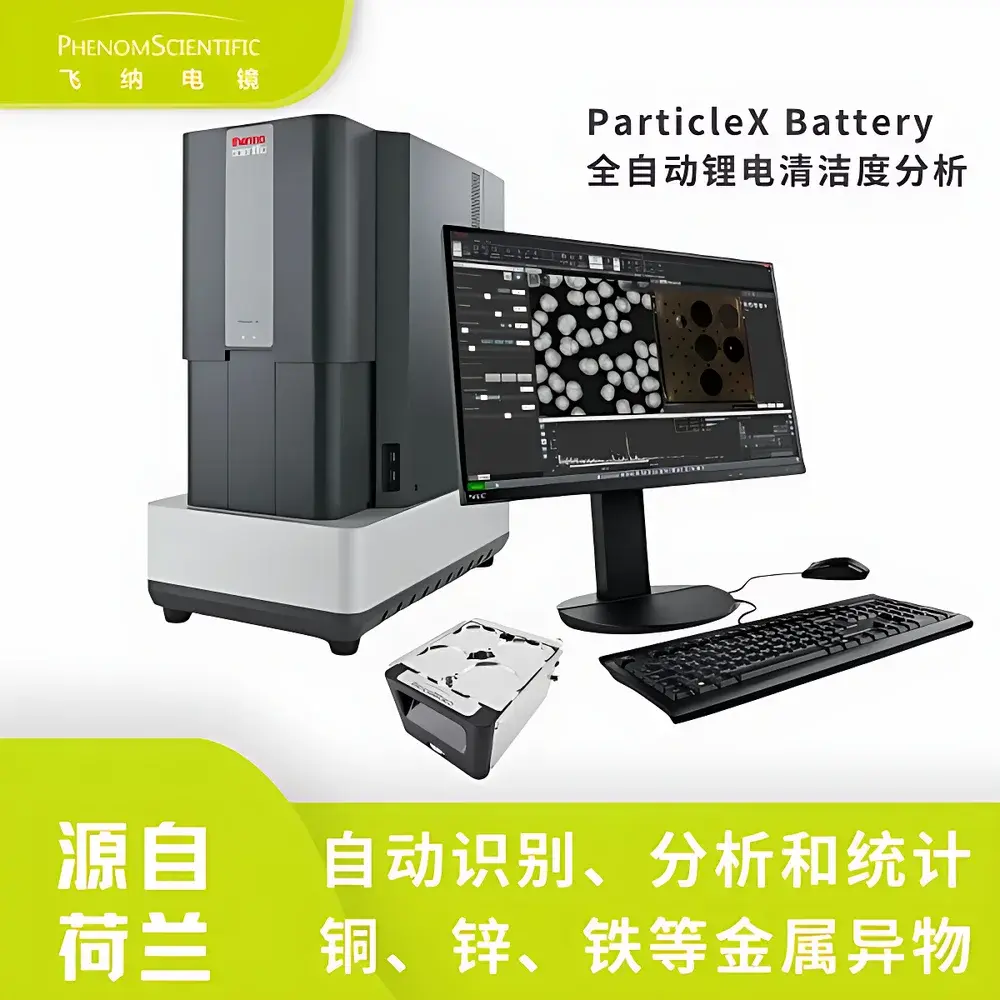
| Brand | Phenom |
|---|---|
| Origin | Netherlands |
| Manufacturer | Phenom-World B.V. |
| Import Status | Imported |
| Model | ParticleX Battery |
| Instrument Type | Benchtop Scanning Electron Microscope (SEM) |
| Electron Source | Cerium Hexaboride (CeB6) |
| Secondary Electron Resolution | 8 nm |
| Maximum Magnification | 200,000× |
| Acceleration Voltage Range | Standard Modes: 2, 5, 10, 15, 20 kV |
| Advanced Mode | Continuously Adjustable from 4.8 kV to 20.5 kV |
| Backscattered Electron Resolution | 8 nm |
| Maximum Sample Capacity | Up to four 47 mm diameter filter membranes simultaneously |
| Standard Detectors | Backscattered Electron Detector (BSE), Energy-Dispersive X-ray Spectrometer (EDS) |
| Optional Detector | Secondary Electron Detector (SED) |
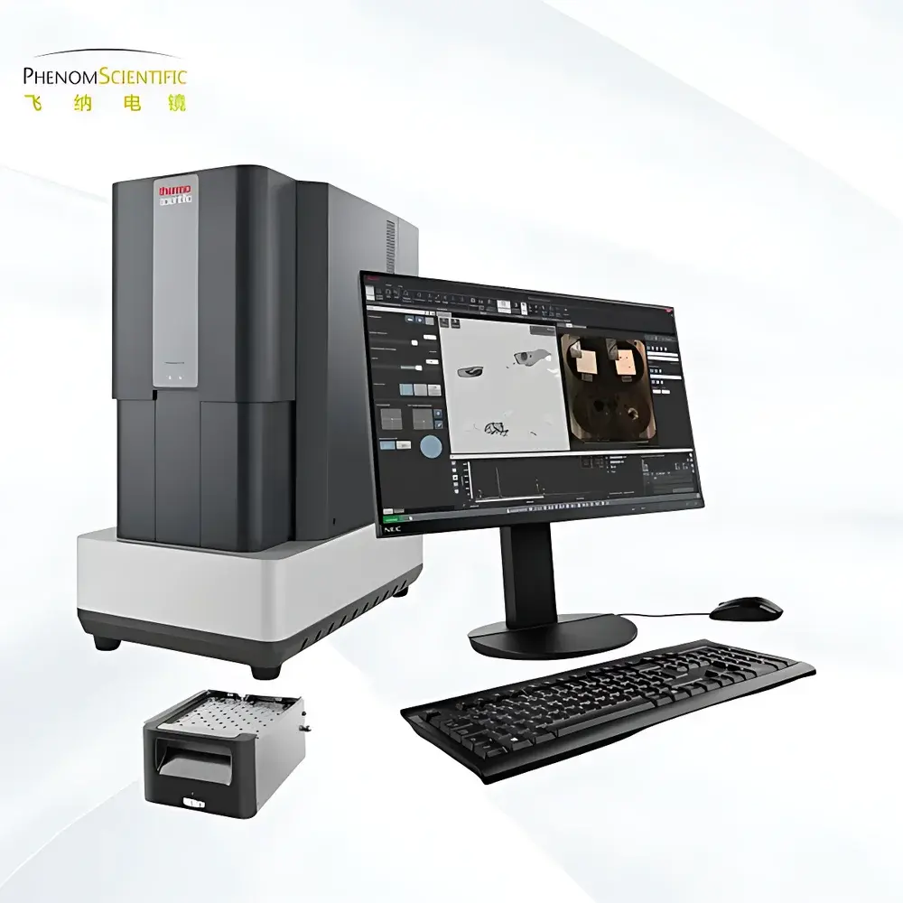
| Brand | Phenom |
|---|---|
| Origin | Netherlands |
| Manufacturer Type | Original Equipment Manufacturer (OEM) |
| Import Category | Imported Instrument |
| Model | ParticleX Battery |
| Instrument Type | Benchtop Scanning Electron Microscope (SEM) |
| Electron Source | Cerium Hexaboride (CeB₆) |
| Secondary Electron Resolution | 8 nm |
| Maximum Magnification | 200,000× |
| Accelerating Voltage Range | Standard Modes: 2 kV, 5 kV, 10 kV, 15 kV, 20 kV |
| Advanced Mode | Continuously Adjustable from 4.8 kV to 20.5 kV |
| Backscattered Electron Resolution | 8 nm |
| Standard Detectors | Backscattered Electron Detector (BSE), Energy-Dispersive X-ray Spectrometer (EDS) |
| Optional Detector | Secondary Electron Detector (SED) |
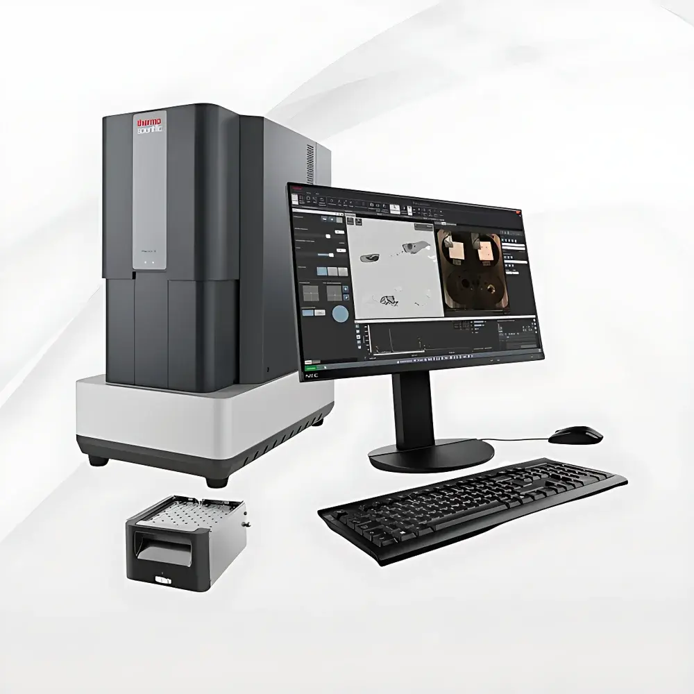
| Brand | Phenom |
|---|---|
| Origin | Netherlands |
| Manufacturer Type | Original Equipment Manufacturer (OEM) |
| Import Status | Imported |
| Model | ParticleX Steel |
| Instrument Type | Benchtop Scanning Electron Microscope |
| Electron Source | Cerium Hexaboride (CeB6) |
| Secondary Electron Resolution | 8 nm |
| Maximum Magnification | 200,000× |
| Accelerating Voltage Range | Standard Modes: 2 kV, 5 kV, 10 kV, 15 kV, 20 kV |
| Advanced Mode | Continuously Adjustable from 4.8 kV to 20.5 kV |
| Backscattered Electron Resolution | 8 nm |
| Standard Detectors | Backscattered Electron Detector (BSE), Energy-Dispersive X-ray Spectrometer (EDS) |
| Optional Detector | Secondary Electron Detector (SED) |
| Brand | Phenom |
|---|---|
| Origin | Netherlands |
| Model | ParticleX Steel Inclusion |
| Instrument Type | Benchtop Scanning Electron Microscope (SEM) |
| Electron Source | Cerium Hexaboride (CeB6) |
| SEM Class | Entry-level Field-Emission Equivalent |
| Secondary Electron Resolution | 8 nm |
| Backscattered Electron Resolution | 8 nm |
| Maximum Magnification | 200,000× |
| Accelerating Voltage Range | Standard Modes: 2, 5, 10, 15, 20 kV |
| Advanced Mode | Continuously Adjustable from 4.8 kV to 20.5 kV |
| Standard Detectors | Backscattered Electron Detector (BSE), Energy-Dispersive X-ray Spectrometer (EDS) |
| Optional Detector | Secondary Electron Detector (SED) |
| Vacuum System | Triple-chamber Separated Architecture |
| Pump-down Time | ≤30 s |
| Stage | High-Precision Motorized Stage |
| Compliance | ASTM E2109, ISO 4967, USP <788>, GB/T 10561 |

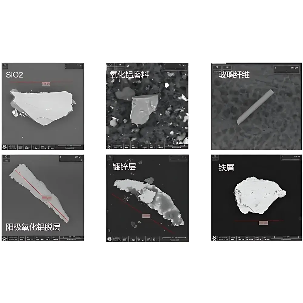
| Brand | Phenom |
|---|---|
| Origin | Netherlands |
| Manufacturer Type | Manufacturer |
| Origin Category | Imported |
| Model | ParticleX TC |
| Instrument Type | Benchtop SEM |
| Electron Source | Cerium Hexaboride (CeB₆) |
| Secondary Electron Resolution | 8 nm |
| Maximum Magnification | 200,000× |
| Acceleration Voltage | Standard Modes: 2 kV, 5 kV, 10 kV, 15 kV, 20 kV |
| Advanced Mode | Continuously Adjustable from 4.8 kV to 20.5 kV |
| Backscattered Electron (BSE) Resolution | 8 nm |
| Max Sample Capacity | Up to four 47 mm diameter filter membranes simultaneously |
| Standard Detector Configuration | Backscattered Electron Detector (BSE), Energy-Dispersive X-ray Spectrometer (EDS) |
| Brand | Phenom |
|---|---|
| Origin | Netherlands |
| Manufacturer | Thermo Fisher Scientific (Phenom brand) |
| Import Category | Imported Instrument |
| Model | ParticleX TC Automotive Cleanliness |
| Instrument Type | Benchtop Scanning Electron Microscope (SEM) |
| Electron Source | Cerium Hexaboride (CeB₆) |
| Secondary Electron (SE) Resolution | 8 nm |
| Maximum Magnification | 200,000× |
| Accelerating Voltage Range | Standard Modes: 2 kV, 5 kV, 10 kV, 15 kV, 20 kV |
| Advanced Mode | Continuously Adjustable from 4.8 kV to 20.5 kV |
| Backscattered Electron (BSE) Resolution | 8 nm |
| Max Sample Capacity | Up to four 47 mm diameter filter membranes simultaneously |
| Standard Detectors | BSE Detector, Energy-Dispersive X-ray Spectrometer (EDS) |
| Optional Detector | Secondary Electron Detector (SED) |