
Scanning Electron Microscope
Filter
Showing 121–150 of 153 results
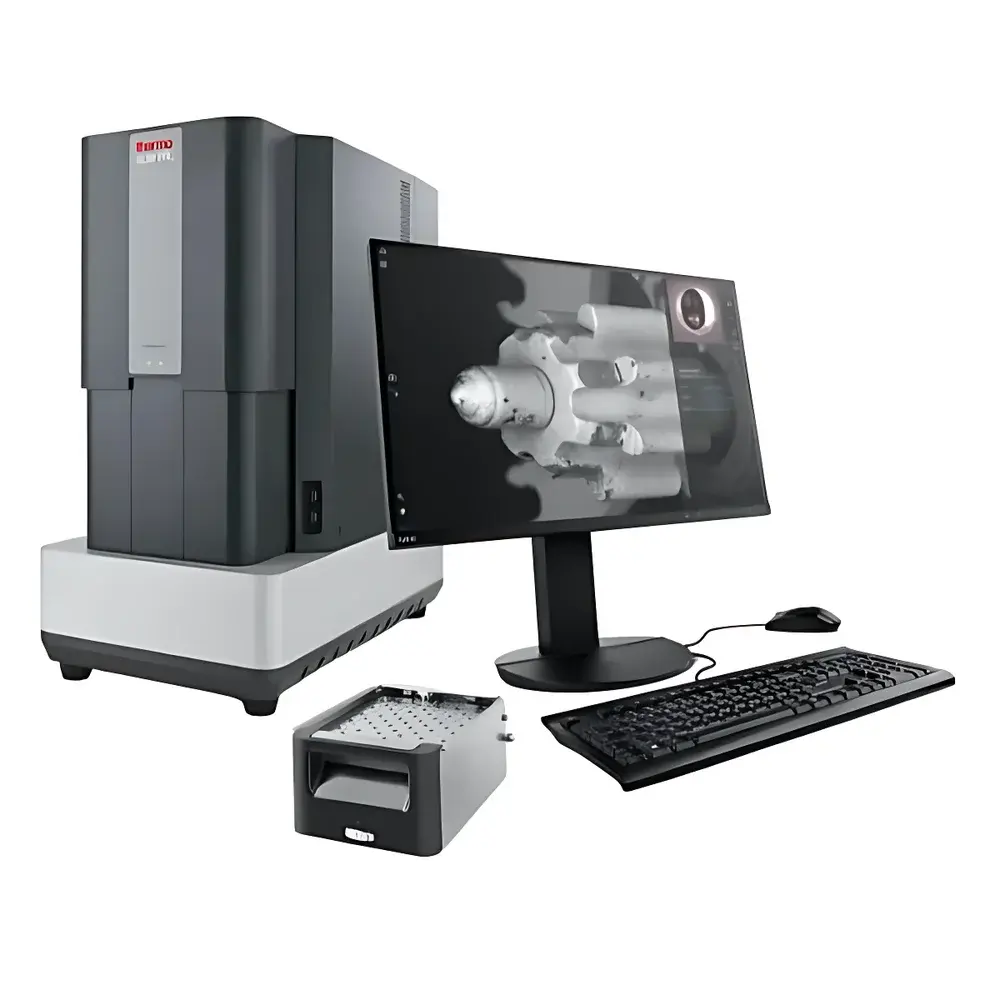
| Brand | Thermo Scientific Phenom |
|---|---|
| Origin | Netherlands |
| Model | Phenom XL G3 |
| Instrument Type | Desktop SEM |
| Electron Source | CeB6 (Cerium Hexaboride) |
| Secondary Electron Resolution | <8 nm |
| Maximum Magnification | 200,000× |
| Accelerating Voltage Range | 4.8–20.5 kV |
| Backscattered Electron Resolution | <8 nm |
| Optional Detectors | EDS, Secondary Electron Detector |
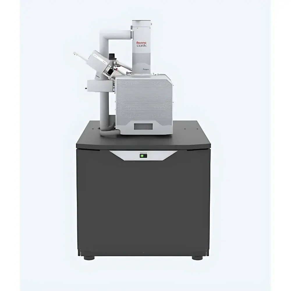
| Brand | Thermo Fisher |
|---|---|
| Origin | Imported (Non-China) |
| Manufacturer Type | Original Equipment Manufacturer (OEM) |
| Electron Gun Type | Cold Field Emission |
| Model | Prisma E SEM |
| Vacuum Modes | High Vacuum, Low Vacuum, Environmental SEM (ESEM) Mode |
| Sample Chamber Capacity | Up to 18 samples per load |
| Detector Flexibility | Multiple detector options including SE, BSE, EDS, and optional STEM-in-SEM |
| Software Integration | ColorSEM real-time elemental mapping, image navigation, customizable UI with Undo/Redo functionality |
| Compliance | Designed for GLP/GMP environments |
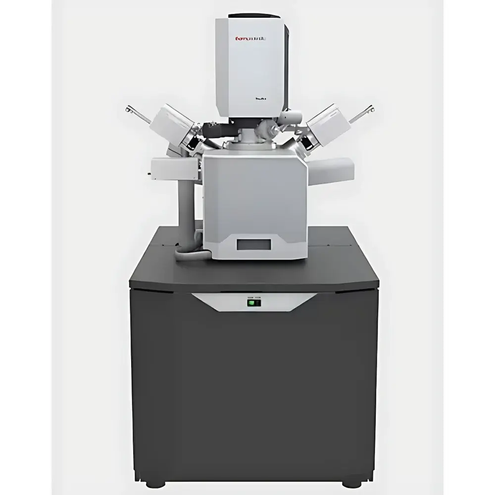
| Brand | Thermo Fisher Scientific |
|---|---|
| Origin | Shanghai, China |
| Model | Quattro ESEM |
| Vacuum Modes | High Vacuum / Low Vacuum / Environmental SEM (ESEM) |
| Resolution | 0.8 nm @ 30 kV (STEM), 1.0 nm @ 30 kV (SE), 3.0 nm @ 1 kV (SE), 1.3 nm @ 30 kV (ESEM/low vacuum) |
| Stage | 5-axis motorized eucentric stage, 105° tilt, 110 × 110 mm² travel |
| Chamber | 340 mm internal width, 12 ports, supports up to three EDS detectors (180° symmetric), co-planar EBSD interface, WDS port |
| Optional In-situ Accessories | -165°C to 1400°C heating/cooling stages, GIS for EBID (Pt, W, C), Peltier stage (-20°C to +60°C), liquid nitrogen cryo-stage, nanomanipulator, multi-probe station |
| Detectors | ETD, LVD, GSED, IR-CCD, Nav-Cam+, DBS, STEM 3+, WetSTEM, RGB-CLD, EDS, EBSD, WDS, Raman, EBIC |
| Software | AutoScript 4 (Python API), Maps, TopoMaps, ChemiSEM (real-time EDS quantification, point/line/map analysis) |
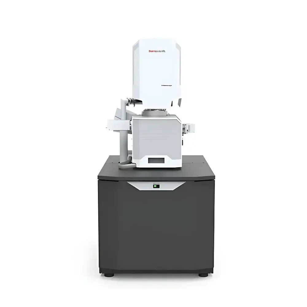
| Brand | Thermo Fisher Scientific |
|---|---|
| Origin | Imported |
| Manufacturer Type | Original Equipment Manufacturer (OEM) |
| Model | Volumescope 2 |
| Instrument Type | Floor-standing SEM |
| Electron Source | Cold Field Emission Gun (CFEG) |
| Accelerating Voltage | 1.0–30 kV |
| Vacuum Modes | High Vacuum (HiVac) and Low Vacuum (LoVac) with VSDBS detector |
| Z-axis Optical Sectioning Resolution | Up to 10 nm |
| Sample Handling | Automated ultramicrotome integration for seamless transition between conventional SEM and SBFI/AT workflows |
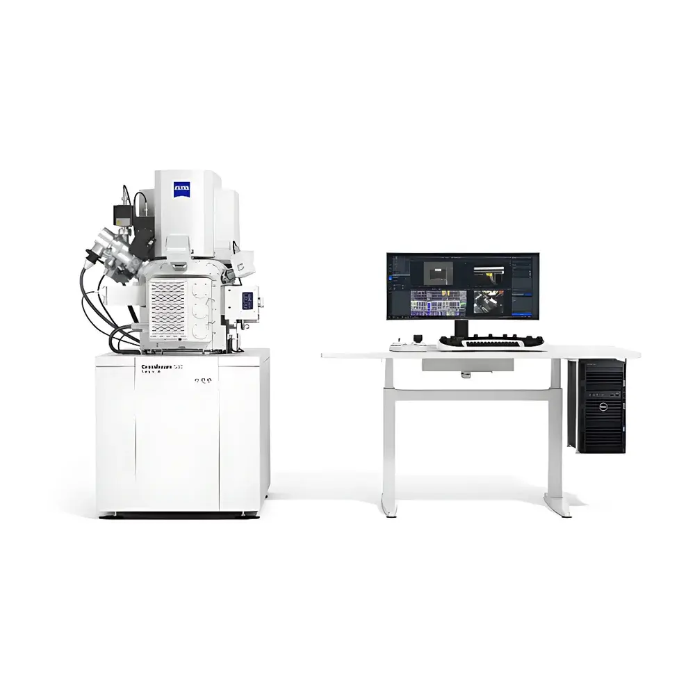
| Brand | ZEISS |
|---|---|
| Origin | Shanghai, China |
| Manufacturer Type | Authorized Distributor |
| Product Origin | Domestic (China) |
| Model | Crossbeam 550 Samplefab |
| Pricing | Upon Request |
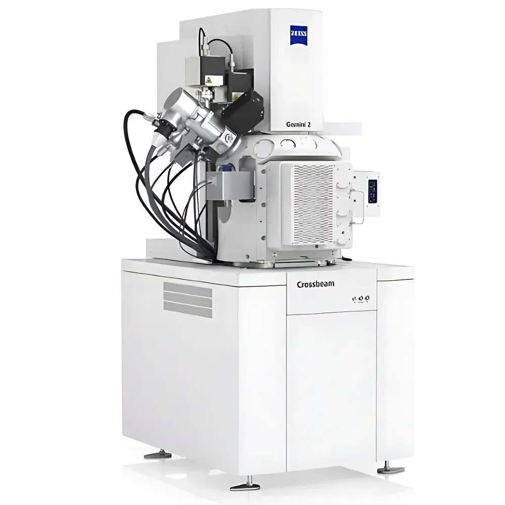
| Brand | ZEISS |
|---|---|
| Origin | Shanghai, China |
| Manufacturer Type | Original Equipment Manufacturer (OEM) |
| Country of Origin | China |
| Model | Crossbeam |
| Instrument Type | Floor-Standing Dual-Beam System |
| Electron Source | Thermal Field-Emission Gun (TFEG) |
| Ion Source | Liquid Metal Gallium (Ga⁺) Focused Ion Beam (FIB) |
| Optional Add-on | Femtosecond Laser Ablation Module |
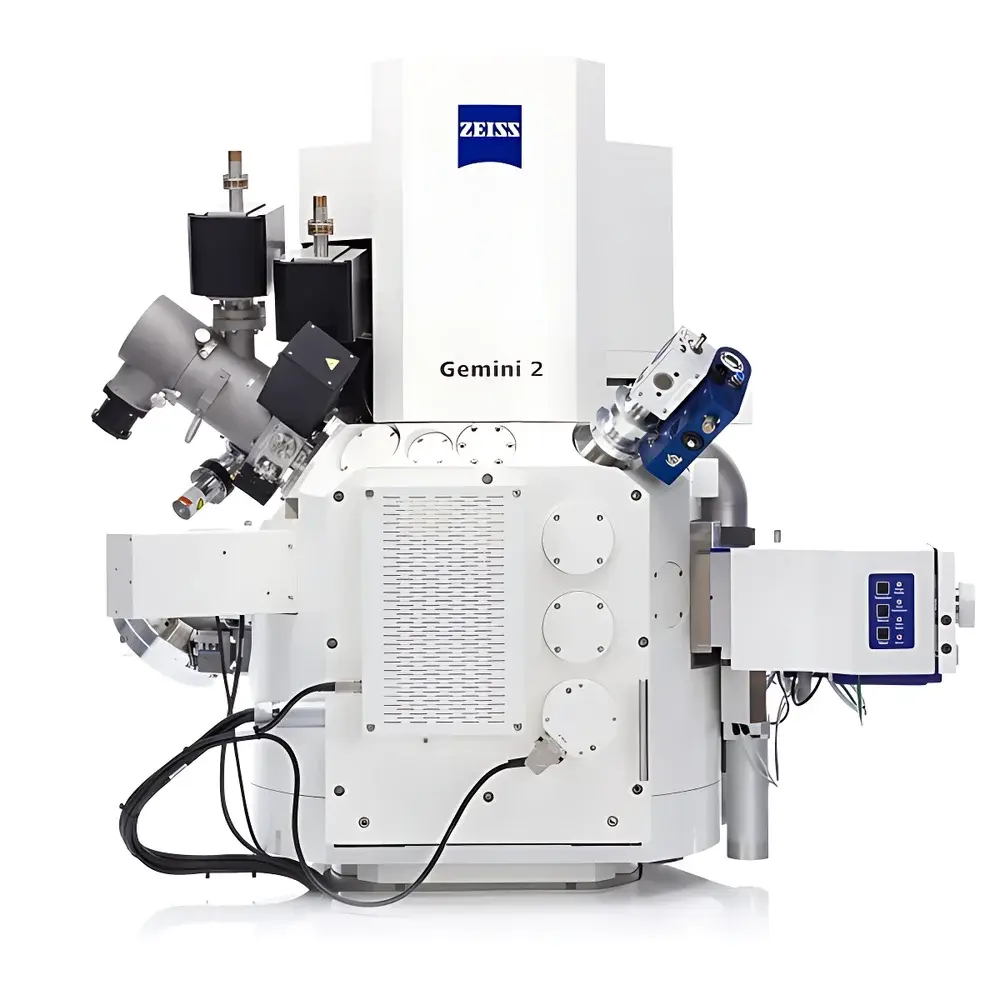
| Brand | ZEISS |
|---|---|
| Origin | Germany |
| Instrument Type | Floor-standing DualBeam System |
| Electron Source | Thermal Field Emission Gun |
| Secondary Electron Resolution | 0.9 nm @ 15 kV (Crossbeam 550), 1.0 nm @ 15 kV (Crossbeam 340) |
| Magnification Range | 12× – 2,000,000× (SEM mode) |
| Acceleration Voltage | 0.02–30 kV (SEM), 0.5–30 kV (FIB) |
| Backscattered Electron Resolution | Not specified |
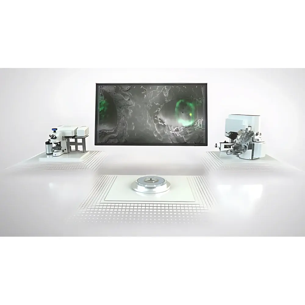
| Brand | ZEISS |
|---|---|
| Origin | Germany |
| Manufacturer Type | Authorized Distributor |
| Import Status | Imported |
| Model | ZEISS Cryo-Correlative Workflow Solution |
| Instrument Form Factor | Floor-standing / Conventional Large-scale |
| Electron Source | Cold Field Emission Gun |
| Secondary Electron Resolution | Not Specified |
| Magnification Range | Not Specified |
| Accelerating Voltage | Not Specified |
| Backscattered Electron Resolution | Not Specified |
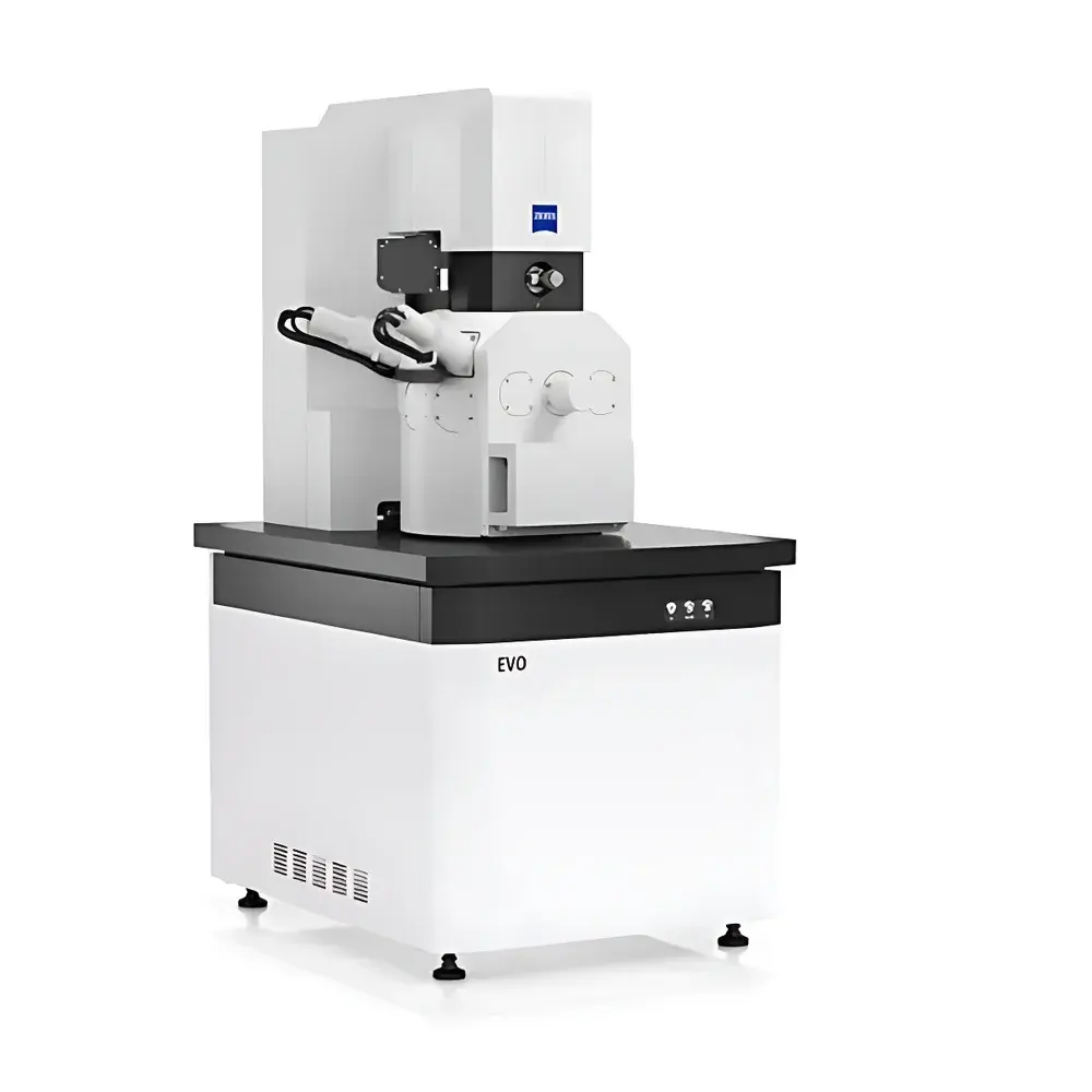
| Brand | ZEISS |
|---|---|
| Origin | Shanghai, China |
| Manufacturer Type | Manufacturer |
| Regional Classification | Domestic |
| Model | EVO |
| Quotation | Upon Request |
| Instrument Form Factor | Floor-standing / Conventional Large-scale |
| Electron Source Type | Tungsten Filament |
| SEM Category | Entry-level Tungsten-Filament SEM |
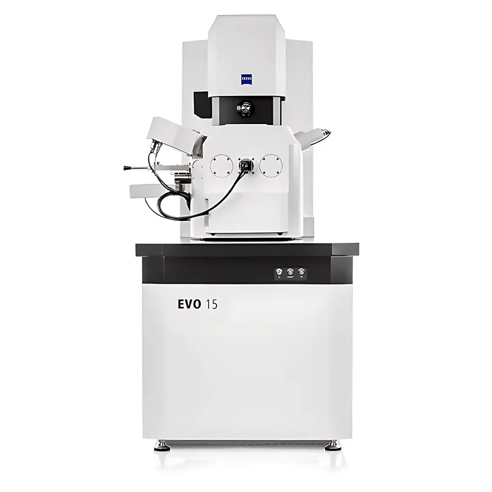
| Brand | ZEISS |
|---|---|
| Origin | Germany |
| Manufacturer Type | Authorized Distributor |
| Origin Category | Imported |
| Model | EVO |
| Pricing | Upon Request |
| Brand | ZEISS |
|---|---|
| Origin | Germany |
| Manufacturer Type | Authorized Distributor |
| Origin Category | Imported |
| Model | EVO |
| Pricing | Available Upon Request |
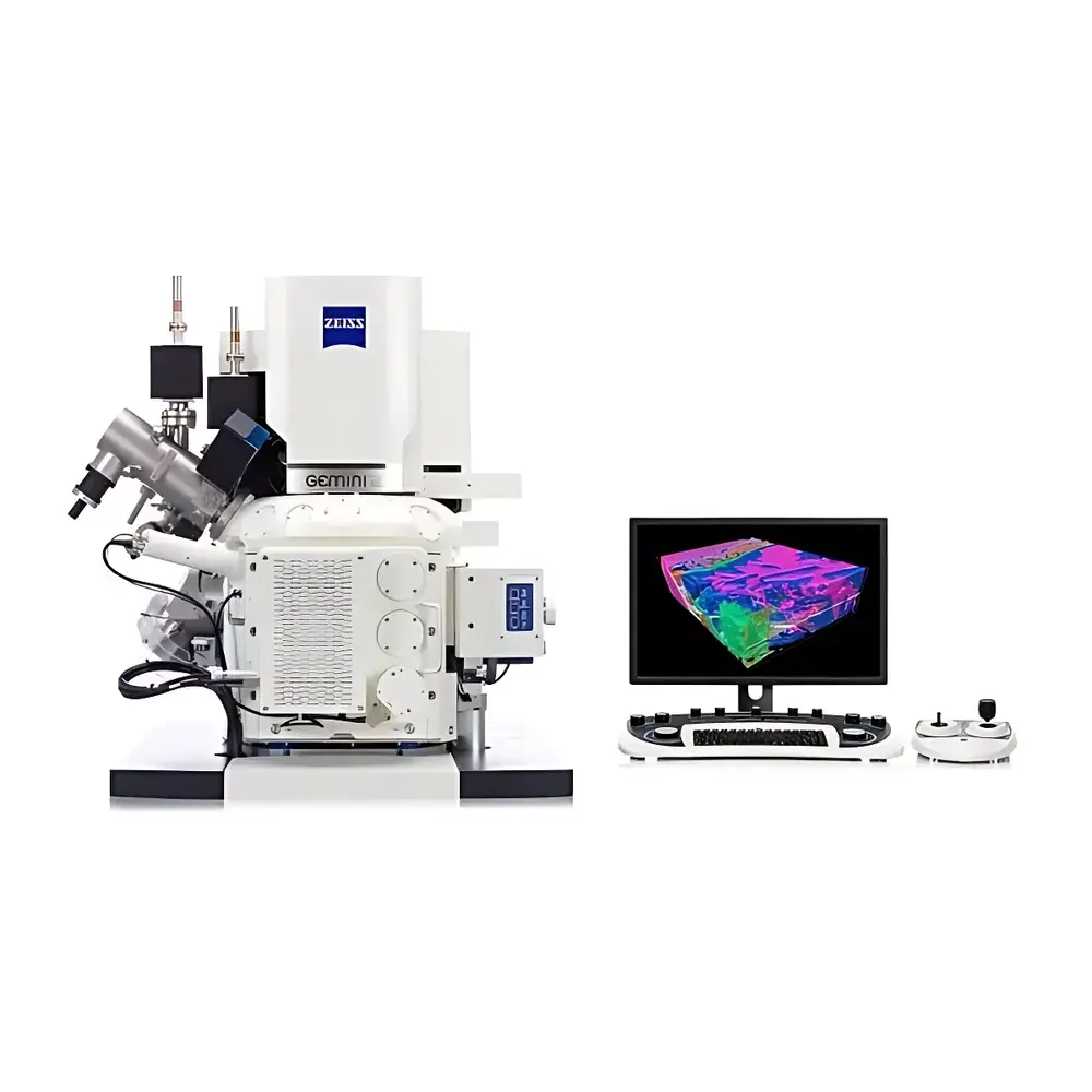
| Brand | ZEISS |
|---|---|
| Origin | Germany |
| Model | EVO10 |
| Instrument Type | Floor-Standing SEM |
| Electron Source | Tungsten Filament |
| Secondary Electron Resolution | 3 nm at 30 kV |
| Magnification Range | 10× to 1,000,000× |
| Accelerating Voltage | 0.2–30 kV |
| Maximum Sample Dimensions | Ø220 mm × 100 mm (H) |
| Stage Travel | X = 80 mm, Y = 100 mm, Z = 35 mm |
| Standard Detectors | Everhart-Thornley Secondary Electron Detector (SED), Solid-State Backscattered Electron Detector (BSE) |
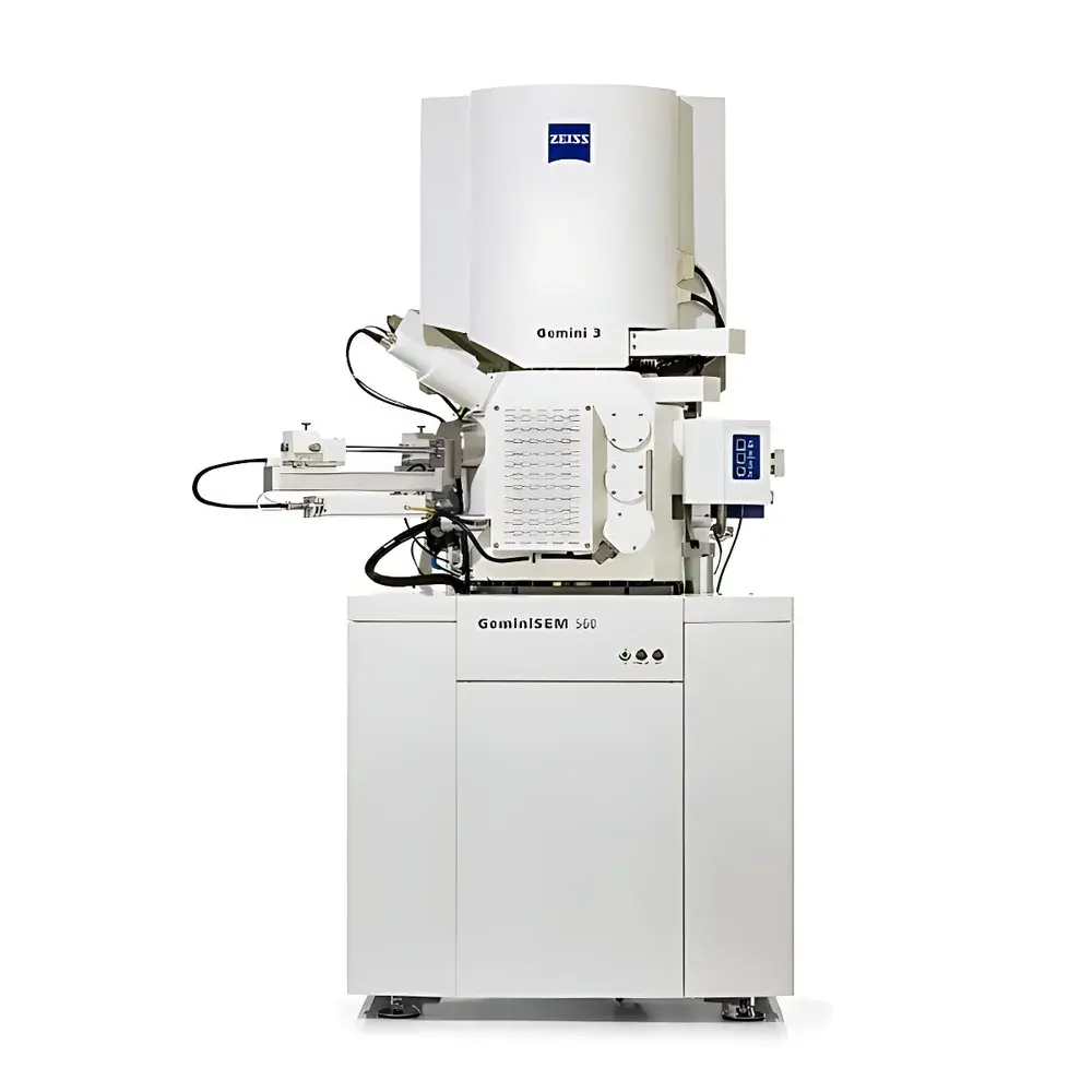
| Brand | ZEISS |
|---|---|
| Origin | Germany |
| Instrument Type | Floor-standing / Conventional Large-format SEM |
| Model | Gemini |
| Key Features | High-efficiency in-lens detection |
| Sample compatibility | Conductive & non-conductive, magnetic & non-magnetic, bulk & coated specimens |
| Compliance | Designed for ISO/IEC 17025-compliant labs |
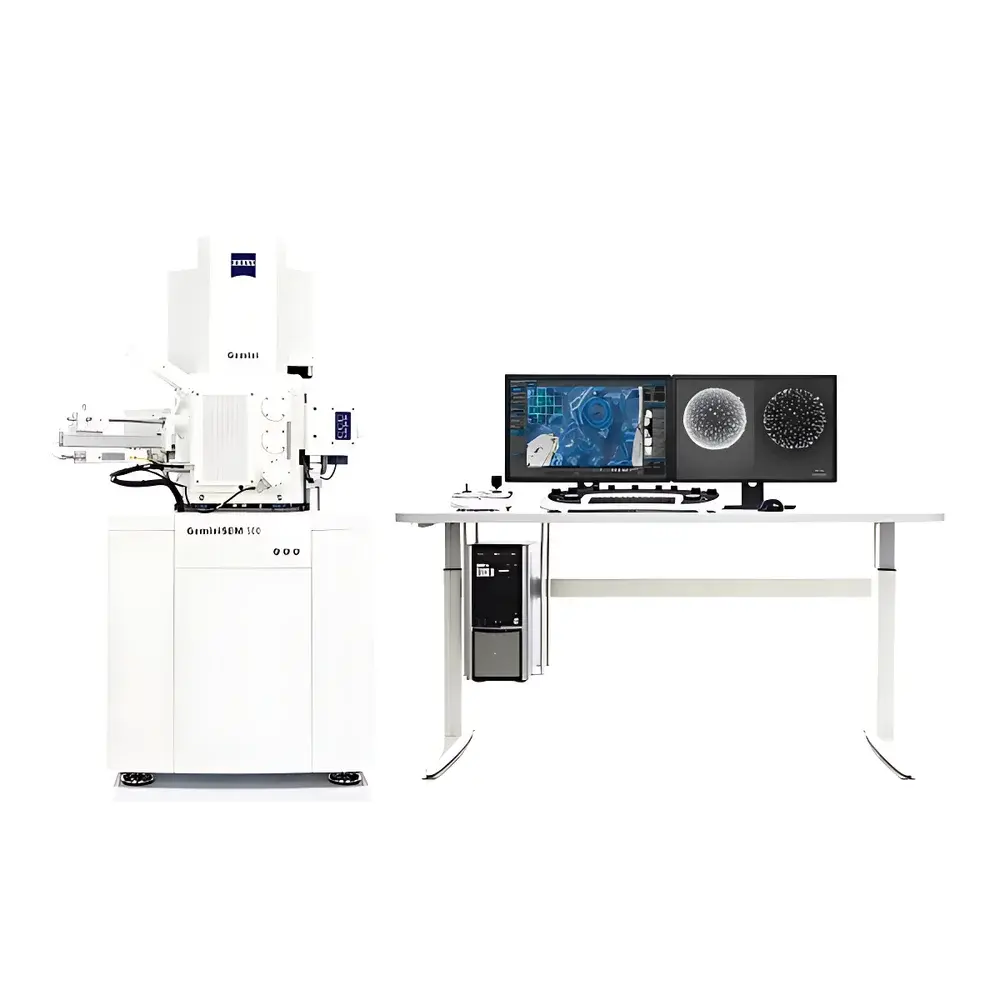
| Brand | ZEISS |
|---|---|
| Origin | Germany |
| Instrument Type | Floor-standing SEM |
| Electron Gun | Cold Field Emission (CFEG) |
| Secondary Electron Resolution | 0.5 nm @ 15 kV, 0.8 nm @ 1 kV (with Tandem Decel) |
| Magnification Range | 50× – 2,000,000× |
| Accelerating Voltage | 0.02 – 30 kV |
| Backscattered Electron Resolution | 1.0 nm @ 1 kV (ESB detector) |
| Detector Configuration | In-lens SE, ET-SE, optional ESB, aSTEM-4, EDS, EBSD, CL |
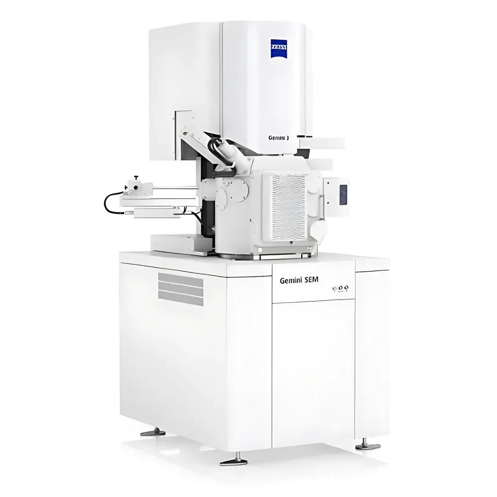
| Brand | ZEISS |
|---|---|
| Origin | Shanghai, China |
| Manufacturer Type | Original Equipment Manufacturer (OEM) |
| Country of Origin | China |
| Model | GeminiSEM |
| Instrument Form Factor | Floor-standing |
| Electron Source | Thermal Field Emission Gun (TFEG) |
| Pricing | Upon Request |
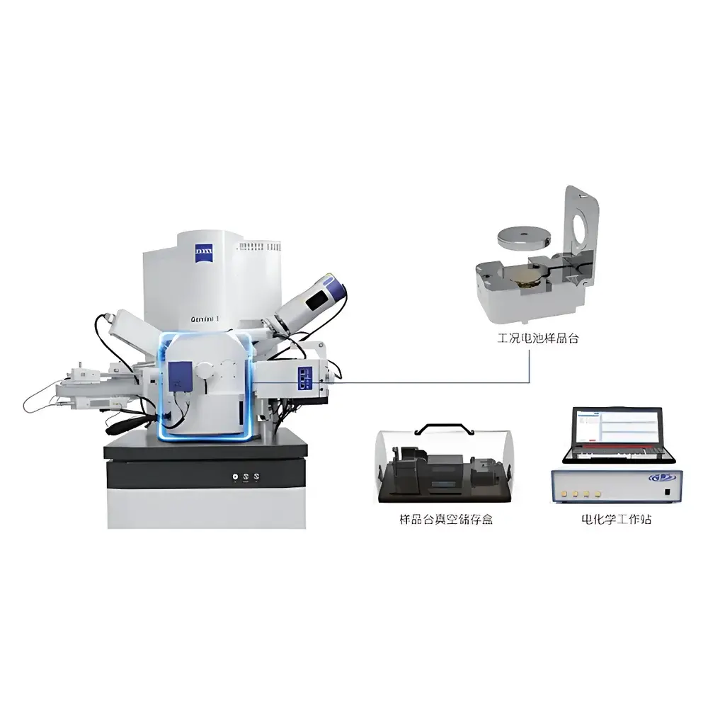
| Brand | ZEISS |
|---|---|
| Origin | Germany |
| Model | In Situ Liquid Electrochemistry Solution |
| Application | Real-time, high-resolution SEM imaging and multimodal analysis of electrochemical cells under operational conditions |
| Key Components | MEMS-based liquid cell chip, custom in situ battery stage, integrated electrical feedthroughs, 10 nm electron-transparent SiN window |
| Compatibility | Standard ZEISS GeminiSEM and SIGMA SEM platforms |
| Compliance | Designed for GLP-compliant workflows |
| Brand | ZEISS |
|---|---|
| Origin | Germany |
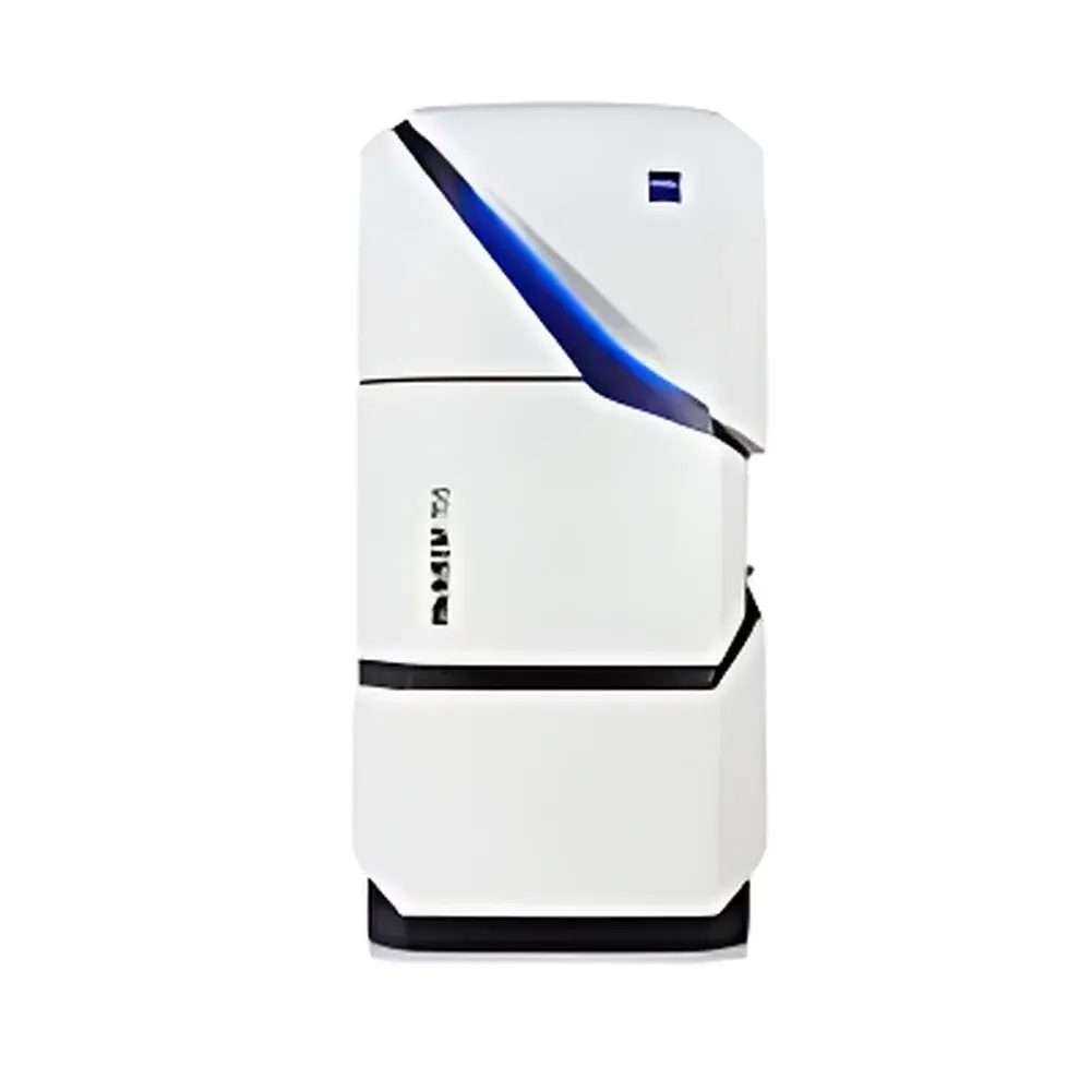
| Model | MultiSEM 706 |
| Beam Count | 91 parallel electron beams |
| Imaging Speed | ~1.5 s per 132 μm × 114 μm hexagonal field of view |
| Resolution | Nanoscale (sub-5 nm typical at 1–3 kV) |
| Sample Capacity | Up to 100 mm wafers or large biological tissue blocks (e.g., 1 mm³ human cortical tissue) |
| Application Scope | High-throughput volumetric EM for semiconductor metrology, connectomics, and materials science |
| Compliance | Designed for integration into GLP/GMP-adjacent workflows |
| Brand | ZEISS |
|---|---|
| Origin | Germany |
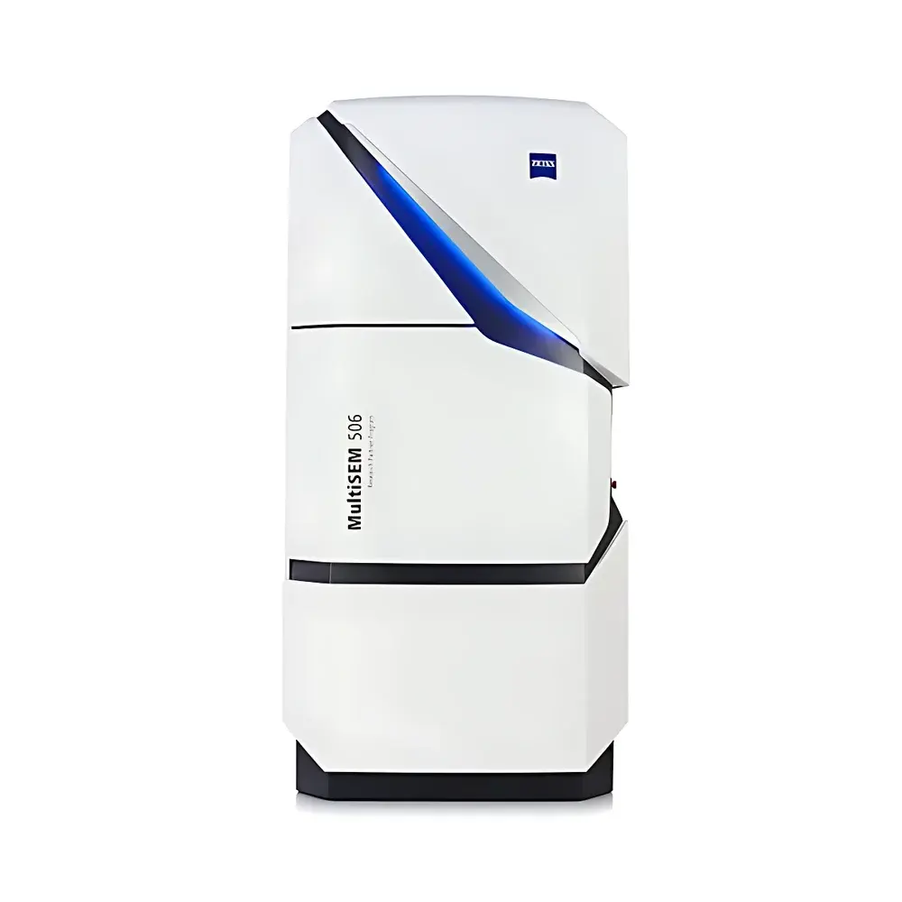
| Model | MultiSEM |
| Electron Beam Configuration | Hexagonal array of 91 beams |
| Landing Energy Range | 1.0–3.0 kV |
| Average Resolution (all beams) | ≤ 3.5 nm @ 1.0 / 1.5 / 3.0 kV |
| Resolution Uniformity | ≤ ±1 nm @ 1.0 / 1.5 / 3.0 kV and 12 µm pitch |
| Beam Pitch Options | 12 µm (standard), 15 µm (optional) |
| Pitch Uniformity | ≤ ±1% |
| Field of View (hexagonal long axis) | 132 µm (12 µm pitch) or 165 µm (15 µm pitch) |
| Per-Beam Current | ≥ 570 pA |
| Total Probe Current | ≥ 52 nA |
| Current Uniformity | ≤ +10% |
| Electron Source | Schottky field-emission gun |
| Filament Current Stability | ≤ 1% per hour |
| Beam Blanking | Electrostatic |
| Working Distance | 1.4 mm |
| Detector System | High-efficiency multi-channel secondary electron detection with projection optics |
| Maximum Scan Rate per Beam | 20 MHz |
| Pixel Size Range | 2–20 nm (12 µm pitch) |
| Image Stitching | Fully automated, 91-subimage hexagonal tiling with adjustable overlap |
| Stage Type | Precision stepper stage |
| Stage Travel (X/Y/Z) | 100 / 100 / 30 mm |
| Stage Repeatability (XY) | ≤ ±3 µm |
| Sample Exchange Time (with exchange chamber) | ≤ 5 min |
| Sample Dimensions (max) | 100 × 100 mm² (XY), ≤ 30 mm height, ≤ 0.2 kg mass, surface flatness ≤ 500 nm P–P over 100 µm |
| Vacuum System | Turbo-molecular pump (>260 L/s) + oil-free scroll pump |
| Control Hardware | ≥4-core 64-bit CPU, ≥32 GB DDR RAM, ≥1 TB HDD, dual 1 Gbit Ethernet |
| OS | Windows 10 (64-bit) |
| Image Acquisition Nodes | 12 rack-mounted computers (≥4-core 64-bit CPU, ≥32 GB DDR3, 1 Gbit + 10 Gbit Ethernet) |
| Software Platform | ZEN core interface with Shuttle & Find, API for custom workflow integration, distributed acquisition database, automated focus/astigmatism/detector balancing, ROI-driven auto-sectioning, continuous serial sectioning workflows, real-time system health monitoring (vacuum, alignment, beam stability) |
| Brand | ZEISS |
|---|---|
| Origin | Germany |
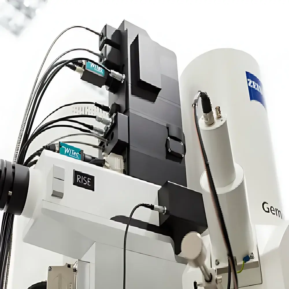
| Model | Sigma 360 |
| Instrument Type | Floor-standing High-Resolution FE-SEM |
| Electron Source | Thermal Field Emission Gun (TFEG) |
| Secondary Electron Resolution | 0.9 nm @ 15 kV, 1.3 nm @ 1 kV |
| Magnification Range | 10× – 1,000,000× |
| Accelerating Voltage | 0.02 – 30 kV |
| Maximum Sample Diameter | ≤ 179 mm |
| Stage | 5-Axis Motorized Eucentric Stage |
| Standard Detectors | In-Lens SE Detector, Everhart-Thornley SE Detector, Solid-State Backscattered Electron (BSE) Detector |
| Brand | ZEISS |
|---|---|
| Origin | Germany |
| Manufacturer Type | Authorized Distributor |
| Origin Category | Imported |
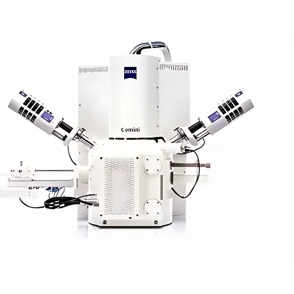
| Model Series | SIGMA |
| Instrument Type | Desktop SEM |
| Electron Gun Type | Cold Field Emission |
| Microscope Class | High-Resolution Field Emission SEM |
| Secondary Electron (SE) Image Resolution | 1.0 nm @ 1 kV, 0.8 nm @ 3 kV |
| Maximum Magnification | 1,000,000× |
| Accelerating Voltage Range | 0.02–30 kV |
| Backscattered Electron (BSE) Image Resolution | 3.0 nm @ 30 kV |
| Working Distance for Analysis | 8.5 mm |
| Tilt Angle for EDS Collection | 35° |
| Variable Pressure Mode | Yes (C2D & VP-SE Detectors) |
| In-Lens SE/BSE Dual Detection | Yes |
| STEM-in-SEM Capability | Yes (aSTEM Detector Optional) |
| EDS Integration | SmartEDX (Si(Li)/SDD, Nitride Window Optimized for Light Elements) |
| RISE Integration | Yes (Fully Integrated Confocal Raman Imaging) |
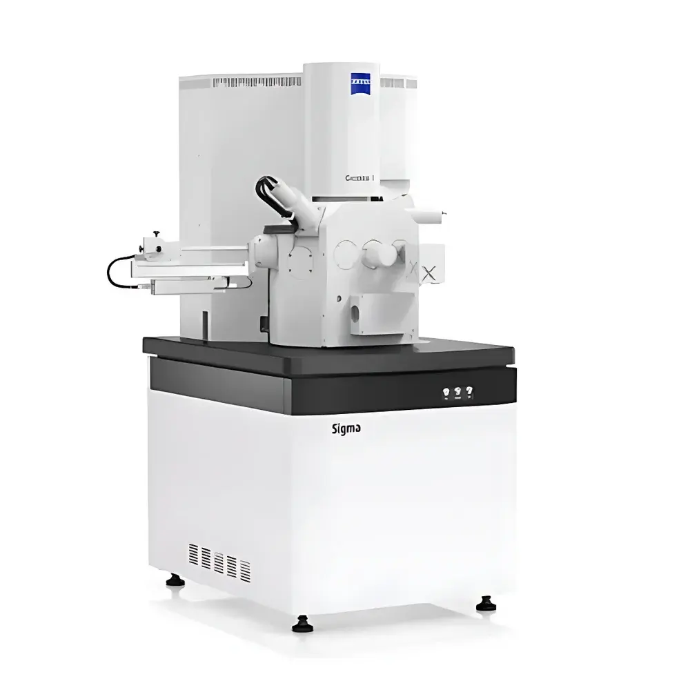
| Brand | ZEISS |
|---|---|
| Origin | Shanghai, China |
| Manufacturer Type | Original Equipment Manufacturer (OEM) |
| Regional Classification | Domestic (China-made) |
| Model | Sigma |
| Pricing | Available Upon Request |
| Instrument Form Factor | Floor-standing / Conventional Large-Format SEM |
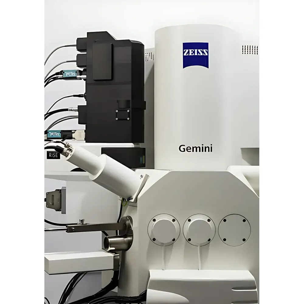
| Brand | ZEISS |
|---|---|
| Origin | Germany |
| Model | SIGMA |
| Detector Options | InLens SE, ETSE, aBSD, Sense BSD |
| EDS Geometry | Optimized for High-Solid-Angle Collection |
| Operating Modes | NanoVP Lite, High-Resolution SEM, Low-Voltage Imaging, In-Situ Compatible |
| Vacuum System | Differential Pumping with Dual-Stage Turbo-Molecular Pumps |
| Stage | Motorized 5-Axis Precision Stage (±0.1 µm repeatability) |
| Beam Control | Gemini II Electron Optics with Active Stigmator and Auto-Alignment |
| Software Platform | SmartSEM with GLP/GMP-Compliant Audit Trail (21 CFR Part 11 Ready) |
| Compliance | ISO 14644-1 Class 5 Cleanroom-Compatible Design, CE Marked, RoHS Compliant |
| Brand | ZEISS |
|---|---|
| Origin | Germany |
| Model | Volutome |
| Application | Integrated in-chamber ultramicrotome for serial block-face imaging in field-emission scanning electron microscopy (FE-SEM) |
| Detector | Volume BSD (Backscattered Electron Detector optimized for volumetric surface imaging) |
| Charge Compensation | Patented localized charge compensation system |
| Automation | Unattended operation up to 72 hours |
| Workflow Integration | End-to-end solution from sectioning and imaging to 3D reconstruction and visualization |
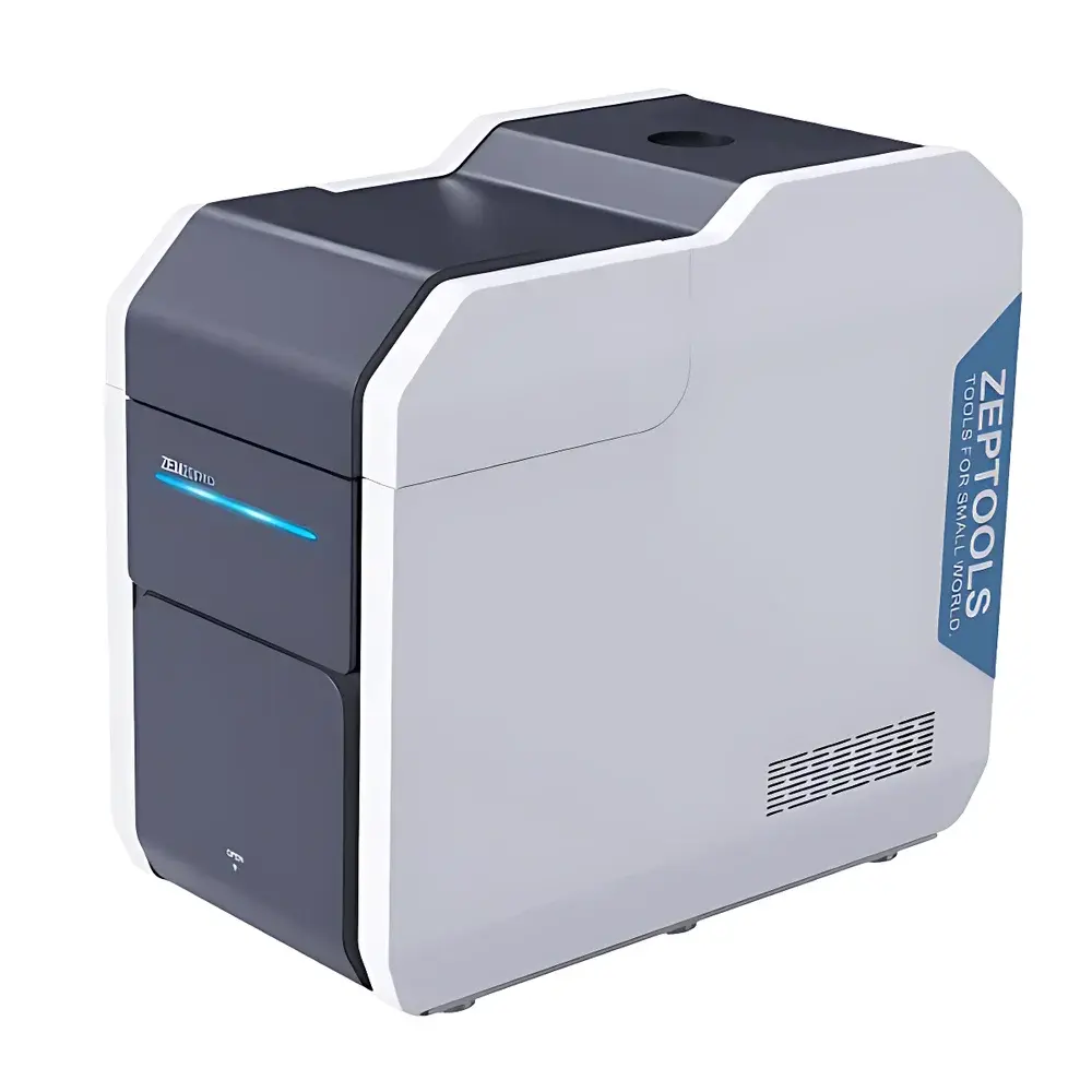
| Brand | ZEPTOOLS |
|---|---|
| Origin | Anhui, China |
| Manufacturer Type | Direct Manufacturer |
| Product Origin | Domestic (China) |
| Model | Custom-Integrated SEM-EDS Platform |
| Price Range | USD 17,000 – 25,500 |
| Magnification Range | 10× – 360,000× (continuously adjustable, user-definable setpoints) |
| Best Imaging Resolution | 3 nm (at 30 kV, SE mode) |
| EDS Detector | Silicon Drift Detector (SDD), ≥10 eV energy resolution (Mn-Kα) |
| Stage Dimensions | 540 mm × 760 mm |
| Motion Axes | 4-axis (X, Y, U, V) motorized precision stage |
| Minimum Positioning Increment | 0.001 mm |
| EDS Quantification Accuracy | ±2–5 wt% (matrix-dependent, per ISO 16529:2014 and ASTM E1508) |
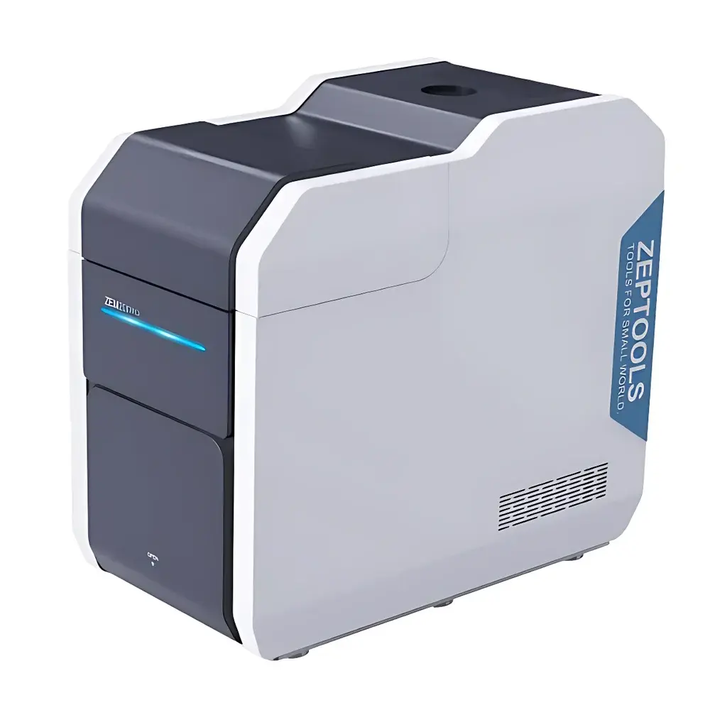
| Brand | ZEPTOOLS |
|---|---|
| Origin | Anhui, China |
| Manufacturer Type | Direct Manufacturer |
| Instrument Type | Desktop SEM |
| Electron Gun | Single-Crystal LaB₆ Filament |
| SEM Class | Entry-Level Tungsten- or LaB₆-Based SEM (Non-FEG) |
| Secondary Electron Resolution | 3 nm @ 20 kV |
| Maximum Magnification | 360,000× |
| Accelerating Voltage Range | 3–20 kV |
| Backscattered Electron Resolution | 3 nm @ 20 kV |
| Sample Chamber Dimensions (max) | 165 × 122 × 51.5 mm (W × D × H) |
| Stage Movement (standard) | X = 60 mm, Y = 55 mm (2-axis) |
| Optional Deceleration Mode | 0–10 kV landing energy via sample bias |
| Imaging Modes | Video mode (512 × 512), Fast Scan (512 × 512), Slow Scan (2048 × 2048) |
| Image Formats | BMP, TIFF, JPEG, PNG |
| Navigation | Integrated optical camera + chamber-viewing CCD |
| Automation | Auto Contrast/Brightness, Auto Focus, Large-Area Image Stitching |
| Dimensions (main unit) | 650 × 370 × 642 mm (W × D × H) |
| In-situ Compatibility | TEC cooling stage, heating stage, tensile stage (ZEPTOOLS proprietary) |
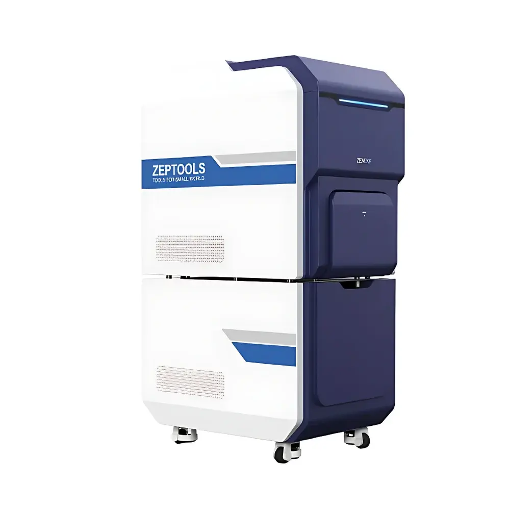
| Brand | ZEPTOOLS |
|---|---|
| Origin | Anhui, China |
| Manufacturer Type | Direct Manufacturer |
| Instrument Type | Desktop SEM |
| Electron Source | Schottky Field Emission Gun |
| Resolution (SE & BSE) | <2.5 nm |
| Max Magnification | 1,000,000× |
| Accelerating Voltage Range | 1–15 kV (continuously adjustable) |
| Stage | Motorized XY (optional XYZ/XYT/5-axis) |
| Detector Options | Secondary Electron (SE), Backscattered Electron (BSE), Energy-Dispersive X-ray Spectroscopy (EDS), Electron Backscatter Diffraction (EBSD) |
| Vacuum System | Triple-stage independent vacuum architecture |
| Imaging Modes | Standard SE/BSE, deceleration mode (0–10 kV sample bias, optional) |
| Image Acquisition | 512×512 (real-time video), 2048×2048 (high-res still capture) |
| Compliance | Designed for ISO/IEC 17025-aligned lab environments |
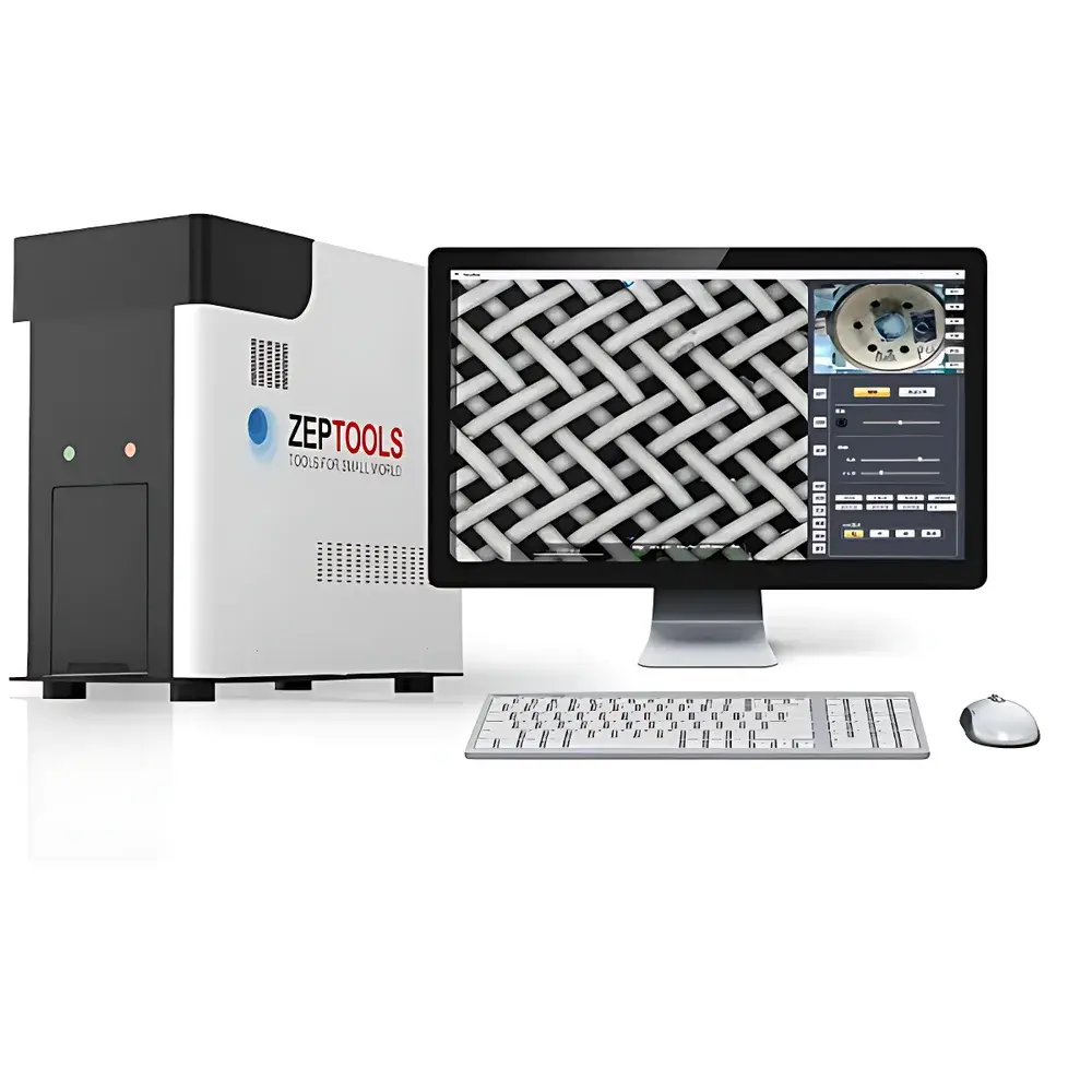
| Brand | ZEPTOOLS |
|---|---|
| Origin | Anhui, China |
| Manufacturer Type | Direct Manufacturer |
| Instrument Type | Desktop SEM |
| Electron Source | Pre-aligned Tungsten Filament |
| Acceleration Voltages | 5 kV / 10 kV / 15 kV |
| Secondary Electron (SE) Resolution | <10 nm |
| Backscattered Electron (BSE) Resolution | <10 nm |
| Maximum Magnification | 150,000× |
| Stage Type | Motorized 2-Axis Sample Stage (X/Y: 25 mm × 25 mm) |
| Vacuum Pumping Time to High Vacuum | ≤2 min |
| Max Sample Dimensions | Ø50 mm × H35 mm |
| Integrated Optics | Monolithic Condenser Lens System |
| Operating Environment | Standard Lab/Office Floor with Vibration Damping Base |
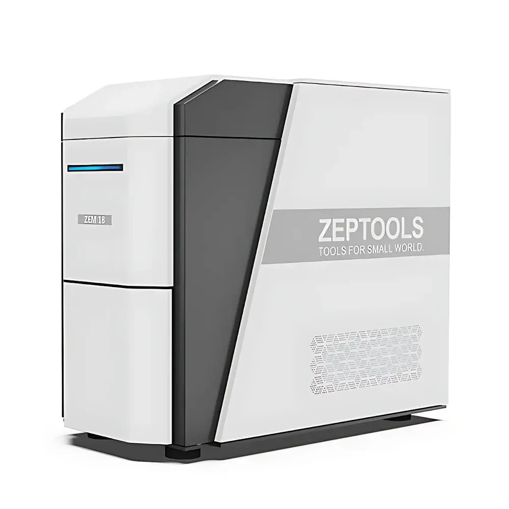
| Brand | ZEPTOOLS |
|---|---|
| Origin | Anhui, China |
| Manufacturer Type | Original Equipment Manufacturer (OEM) |
| Product Category | Domestic |
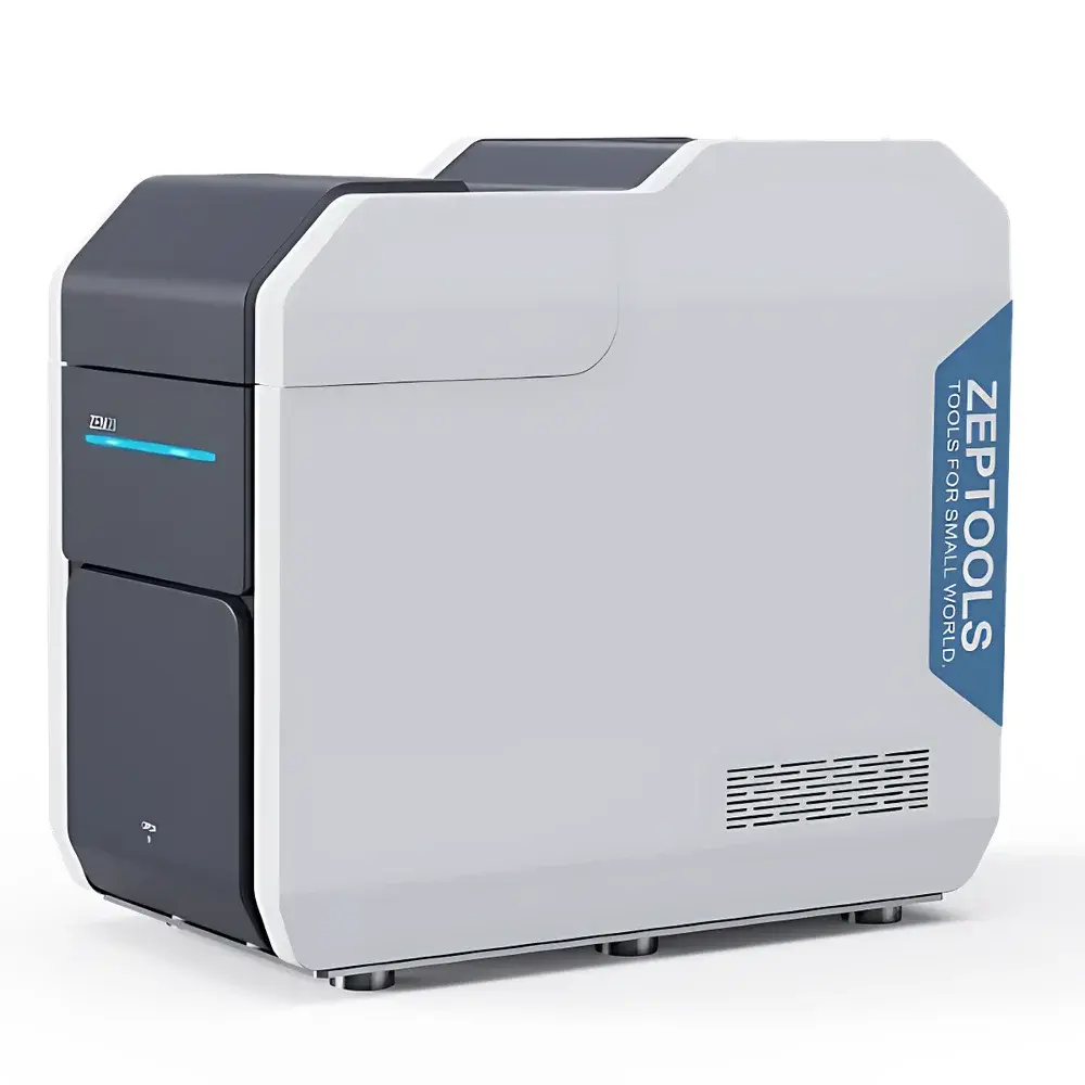
| Model | ZEM18 |
| Instrument Type | Desktop SEM |
| Electron Source | Pre-aligned Tungsten Filament |
| SEM Class | Entry-level Tungsten-Filament SEM |
| Secondary Electron (SE) Resolution | <6 nm |
| Backscattered Electron (BSE) Resolution | <6 nm |
| Maximum Magnification | 200,000× |
| Accelerating Voltage Range | 3–18 kV |
| Maximum Sample Dimensions | Ø50 mm × 35 mm (H) |
| Stage | Motorized 2-Axis Automated Stage |
| Signal Acquisition Bandwidth | 10 MHz |
| Vacuum Mode Options | High Vacuum (<5×10⁻³ Pa), Low Vacuum (optional) |
| Pump-down Time (High Vacuum) | <90 s |
| Imaging Modes | Video Mode, Fast Scan Mode, Slow Scan Mode |
| Auto Functions | Auto Focus, Auto Brightness/Contrast |
| Detector Configurations | SE Detector, BSE Detector, Optional EDS Detector |
| Brand | ZEPTOOLS |
|---|---|
| Origin | Anhui, China |
| Manufacturer Type | Direct Manufacturer |
| Product Origin | Domestic (China) |
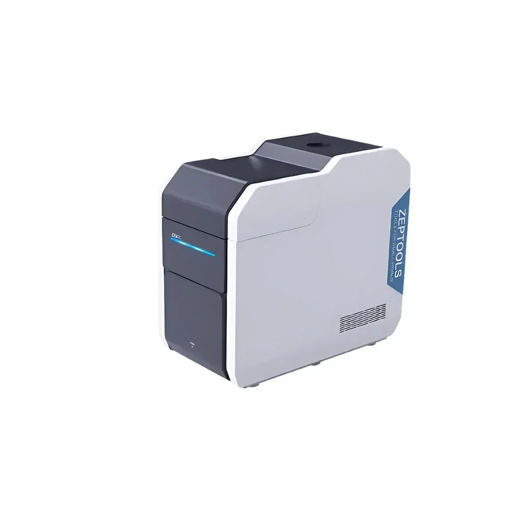
| Model | ZEM20 In-situ Tensile Integrated SEM |
| Instrument Type | Desktop SEM |
| Electron Source | Tungsten Filament |
| SEM Class | Entry-level Tungsten-Filament SEM |
| Secondary Electron (SE) Resolution | 4 nm @ 20 kV |
| Maximum Magnification | 360,000× |
| Accelerating Voltage Range | 3–20 kV (1 kV step adjustment) |
| Backscattered Electron (BSE) Resolution | 4 nm @ 20 kV |
| In-situ Stage Load Capacity | 0–1000 N |
| Displacement Resolution | 20 nm |
| Optional Heating Module | Yes |
| Mechanical Testing Modes | Tensile, Compression, Three-point Bending |
| Vacuum Architecture | Dual-chamber (separated electron gun & specimen chamber) |
| Sample Chamber Camera | Integrated HD in-chamber camera |
| Chamber Volume | Extra-large for multi-modal in-situ platform integration |
| Brand | ZEPTOOLS |
|---|---|
| Origin | Anhui, China |
| Manufacturer Type | Direct Manufacturer |
| Instrument Type | Desktop SEM |
| Electron Source | Pre-aligned Tungsten Filament |
| SEM Class | Entry-level Tungsten-Filament SEM |
| Secondary Electron (SE) Resolution | 4 nm |
| Maximum Magnification | 360,000× |
| Accelerating Voltage Range | 3–20 kV (1 kV step adjustment) |
| Backscattered Electron (BSE) Resolution | 4 nm |
| Stage Option | 5-Axis Motorized Stage (Optional) |
| Chamber Dimensions | 185 mm × 176 mm × 125 mm |
| Vacuum Modes | High Vacuum & Low Vacuum |
| Environmental Suitability | Vibration-isolated design for standard labs/offices/factories |
| Detector Configuration | SE + BSE detectors |
| Optional Upgrades | EDS, Deceleration Mode, In-situ Platforms |
| Filament Upgrade Option | LaB₆ |