
Semiconductor Instruments
Filter
Showing 211–240 of 852 results
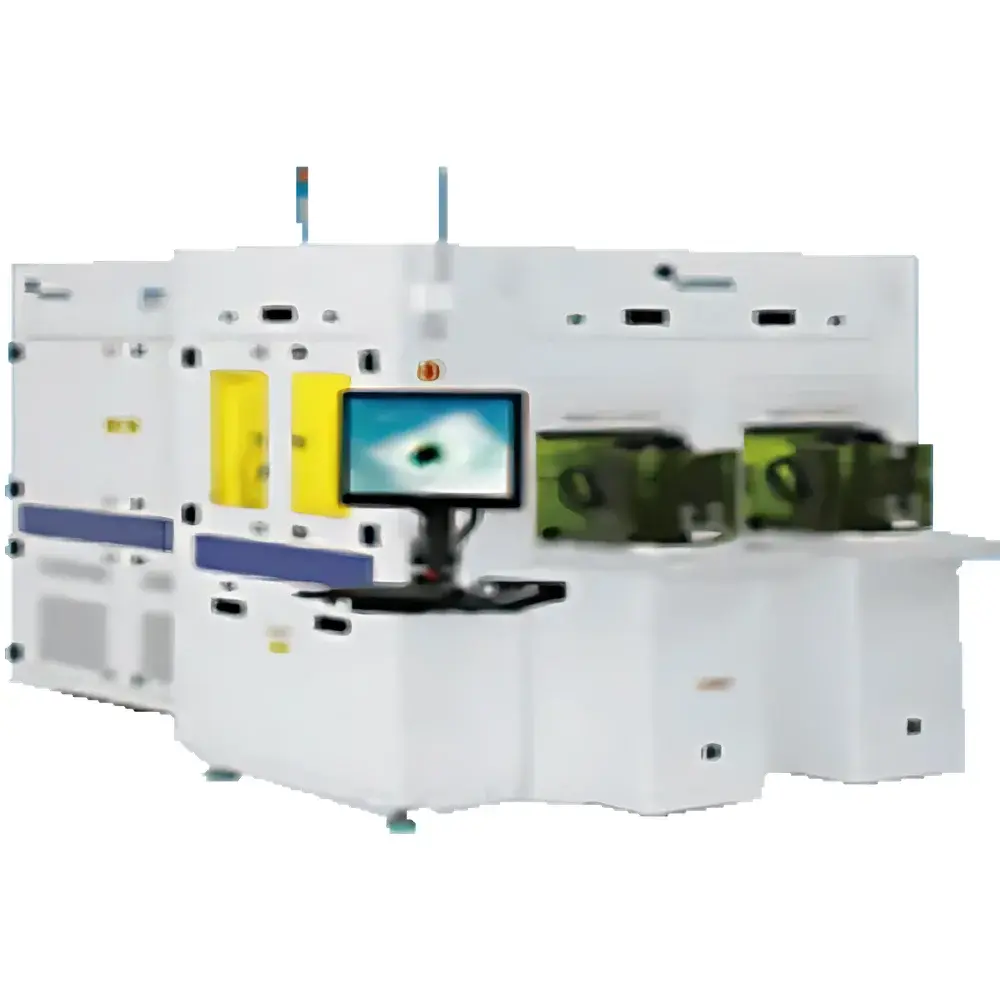
| Origin | Imported |
|---|---|
| Manufacturer Type | Authorized Distributor |
| Model | EagleT-i |
| Price Range | USD 650,000 – 1,050,000 |
| Inspection Speed | Up to 50 million bump measurement points per wafer |
| 2D Detection Accuracy | 0.2 µm |
| 3D Height Measurement Accuracy | 0.05 µm (Measurement Range: 2–100 µm) |
| Minimum Detectable Line Width/Spacing | 2 µm (post-RDL) |
| Defect Detection Limit | 0.2 µm surface anomalies |
| Compatible Substrates | Flat and warped wafers, square dies, compound semiconductor substrates |
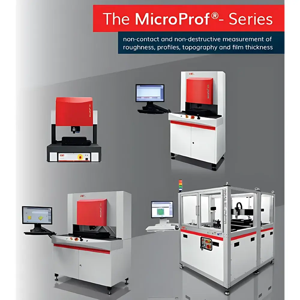
| Brand | Camtek / FRT |
|---|---|
| Origin | Germany |
| Manufacturer Type | Authorized Distributor |
| Import Status | Imported |
| Model | MicroProf®100 |
| Detection Speed | Up to 50 million measurement points per wafer |
| 2D Lateral Resolution | 0.2 µm |
| 3D Vertical Height Accuracy | ±0.05 µm (measuring range: 2–100 µm) |
| Dual-Sided Measurement Capability | Yes (TTV/Bow/Warp/TIR/LTV) |
| Optical Principle | White-light Interferometry & Chromatic Confocal Sensing |
| Optional IR Sensor | Integrated for backside thickness monitoring of Si, GaAs, InP, SiC, GaN wafers |
| Compliance | SEMI Standard-compliant dual-probe architecture |
| Form Factor | Compact benchtop metrology platform |
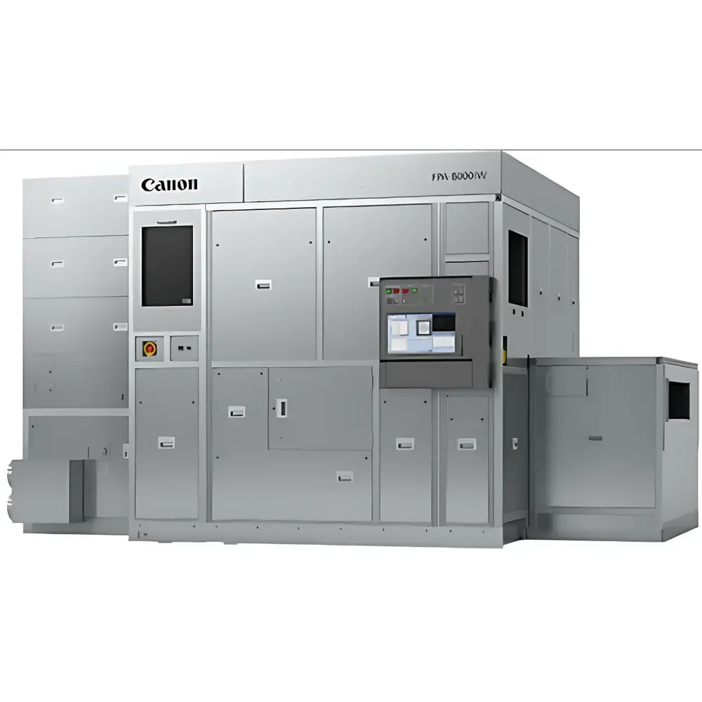
| Brand | Canon (Japan) |
|---|---|
| Origin | Japan |
| Equipment Type | Mask Lithography System (Stepper/Scanner/NIL) |
| Wafer/Substrate Compatibility | 200 mm, 300 mm, Gen 8.6 to Gen 10.5 FPD glass |
| Resolution | ≤65 nm (KrF stepper, with multi-patterning), 0.18–0.35 µm (i-line/KrF), 1–2 µm (packaging), 3–5 µm (FPD), <10 nm (NIL, theoretical) |
| Exposure Source | i-line (365 nm), KrF (248 nm), NIL UV imprint |
| Alignment Accuracy | ±0.5 µm (FPA-5520iV) |
| Throughput | ~100–120 wph (300 mm, FPA-8000 series) |
| Compliance | ISO 14644-1 Class 5 cleanroom compatible, SEMI S2/S8 certified, supports GLP/GMP-aligned process documentation |
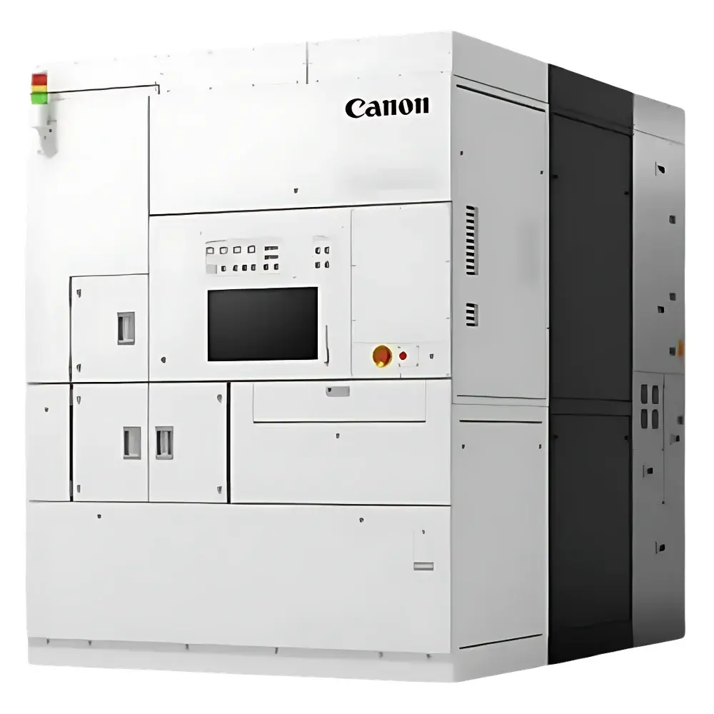
| Brand | Canon |
|---|---|
| Origin | Japan |
| Manufacturer Type | Authorized Distributor |
| Product Origin | Imported |
| Model | FPA5000 ES4 |
| Resolution | 0.13 µm |
| Exposure Wavelength | 248 nm |
| Maximum Exposure Field | 26 mm × 33 mm |
| Numerical Aperture (NA) | 0.5–0.8 |
| Reduction Ratio | 4:1 |
| Overlay Accuracy | ±25 nm |
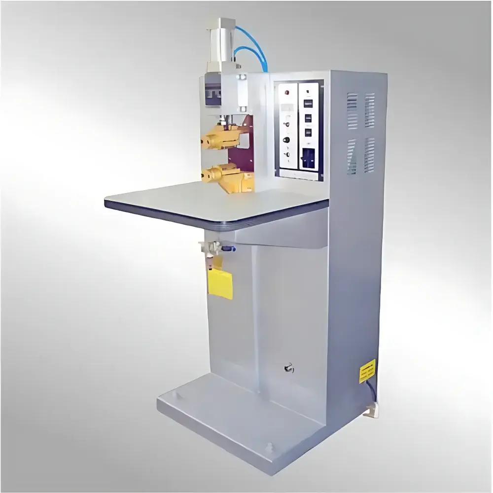
| Brand | Zhengye |
|---|---|
| Origin | Guangdong, China |
| Manufacturer Type | Direct Manufacturer |
| Country of Origin | China |
| Model | PYC500 |
| Pricing | Available Upon Request |
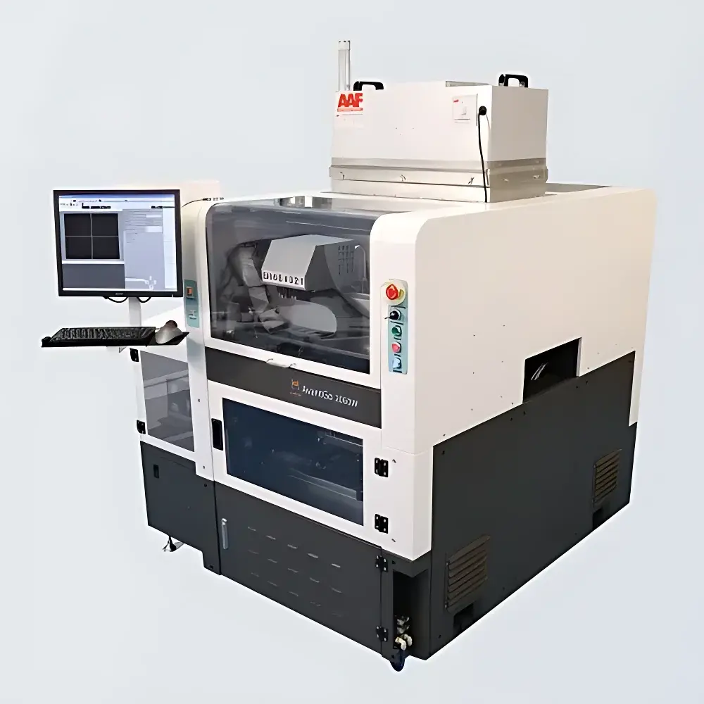
| Brand | Capcon |
|---|---|
| Origin | Beijing, China |
| Manufacturer Type | Authorized Distributor |
| Regional Classification | Domestic (PRC) |
| Model | CAPCON-Die Bonder |
| Pricing | Available Upon Request |
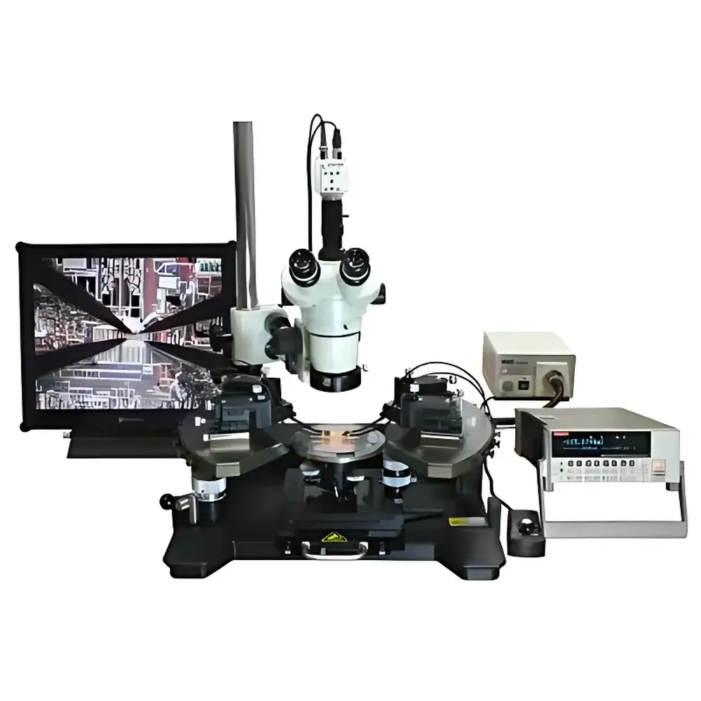
| Origin | USA |
|---|---|
| Manufacturer Type | Authorized Distributor |
| Origin Category | Imported |
| Model | EPS Series |
| Price Range | USD $65,000 – $130,000 (FOB USA) |
| Product Category | RF-Compatible Manual Probe Station |
| Operation Mode | Manual |
| Base Platform | 150 mm Wafer-Capable |
| Max XY Travel | 155 mm × 155 mm |
| Minimum Positioning Resolution | 5 µm |
| Theta Rotation | 360° Continuous |
| Z-Axis Vertical Travel | 10 mm |
| Standard Base Dimensions | 490 mm × 490 mm × 480 mm (W × D × H) |
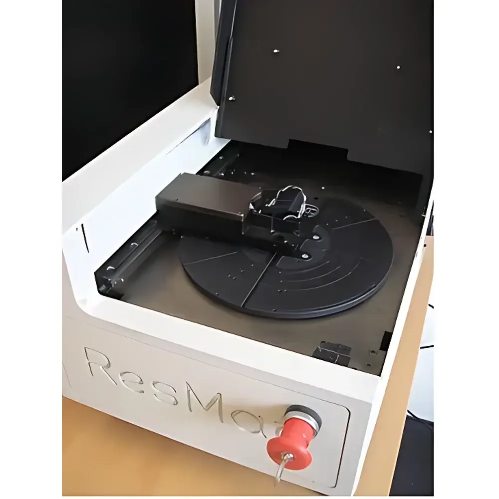
| Brand | CDE ResMap |
|---|---|
| Origin | USA |
| Model | ResMap 168 |
| Automation Level | Fully Automated |
| Probe Material | Tungsten Carbide (WC) |
| Probe Lifetime | >500,000 measurements |
| Vertical Resolution for Probe Contact Optimization | 0.01 mm |
| Measurement Range | 1 mΩ/□ to 5 MΩ/□ |
| Standard Reference Wafers Included | NIST-traceable calibration set (6 pieces) |
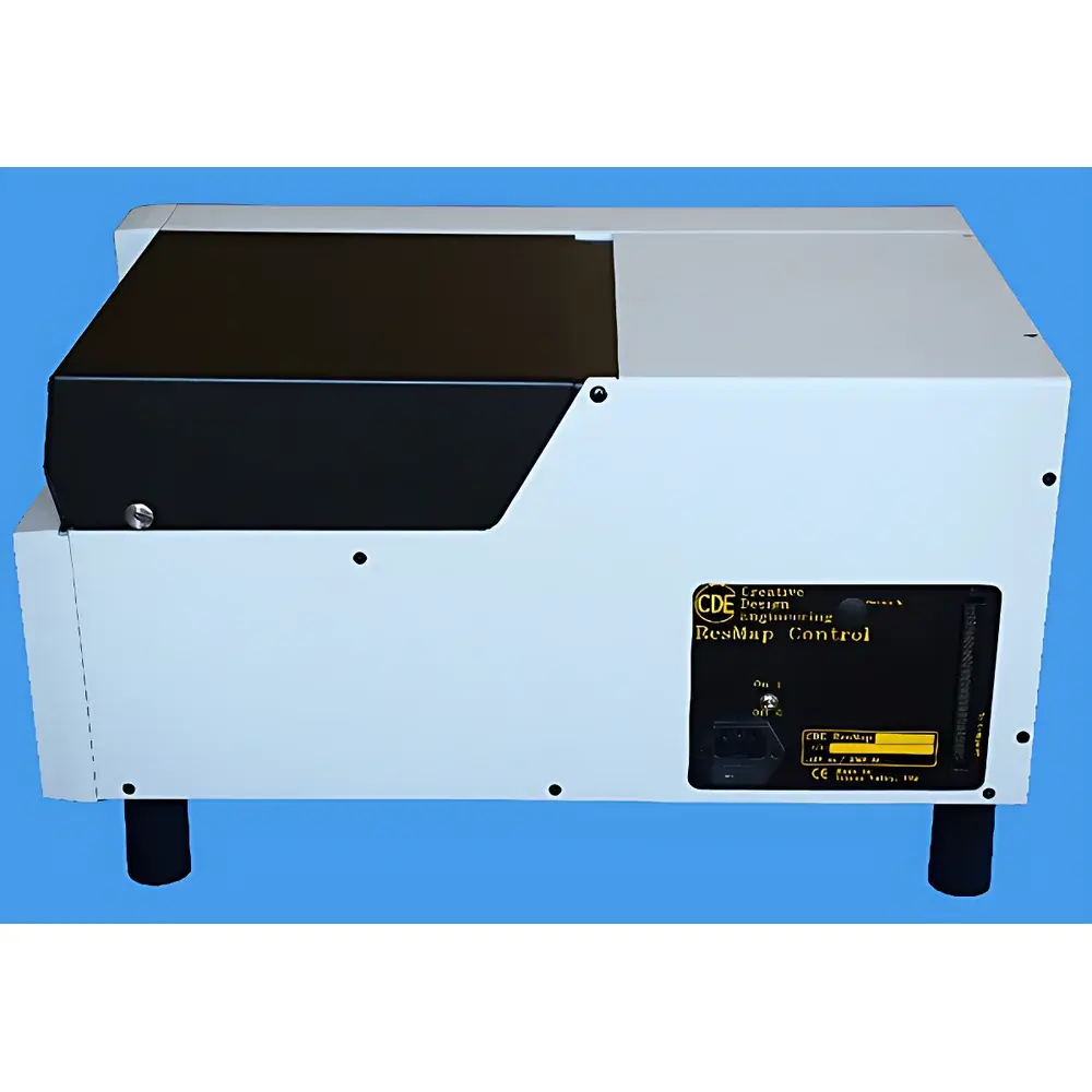
| Brand | CDE (Creative Design Engineering) |
|---|---|
| Model | ResMap 178 |
| Origin | USA |
| Automation Level | Semi-Automatic |
| Measurement Range | 1 mΩ/□ to 5 MΩ/□ |
| Repeatability | ≤ ±0.02% (on static standard resistor) |
| Scan Speed | ≥49 points/min |
| Edge Correction Capability | Effective within 1.5 mm from wafer edge |
| Probe Force Control | Software-adjustable, 90–200 g |
| Probe Types Available | A, B, K, M, N series and custom configurations |
| Supported Substrates | Circular wafers up to 200 mm (8″), square substrates up to 156 mm × 156 mm |
| Data Output | 2D/3D resistivity maps, statistical summaries, Excel-compatible reports |
| Compliance | NIST-traceable calibration standards included (6 certified reference wafers) |
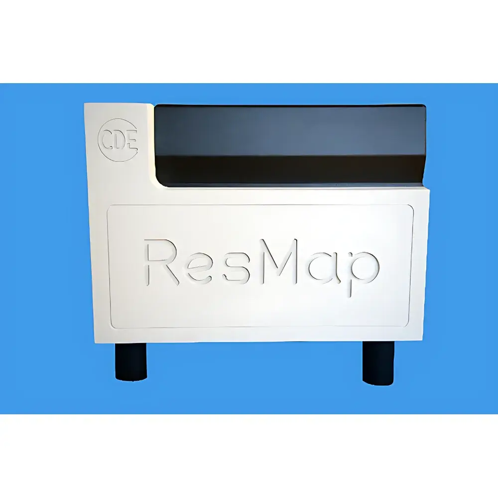
| Brand | CDE ResMap |
|---|---|
| Origin | USA |
| Model | ResMap 273 |
| Automation Level | Fully Automatic |
| Price | USD $68,000 |
| Probe Material | Tungsten Carbide (WC) |
| Probe Lifetime | >500,000 touchdowns |
| Standard Calibration Wafers Included | NIST-traceable set of 6 wafers |
| Measurement Range | 1 mΩ/□ to 5 MΩ/□ |
| Vertical Resolution for Probe Landing Control | 0.01 mm (software-adjustable) |
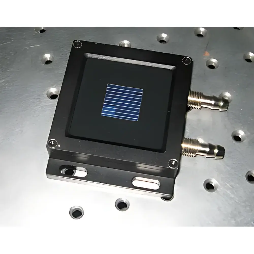
| Brand | CEL |
|---|---|
| Origin | Beijing, China |
| Manufacturer Type | Direct Manufacturer |
| Origin Category | Domestic (China) |
| Model | CEL-RCCO |
| Price | USD 2,800 (FOB Beijing) |
| Active Area | 20 mm × 20 mm |
| Spectral Response Range | 400–1100 nm |
| Calibration Irradiance | 1000 W/m² (AM1.5G) |
| Calibration Temperature | 25 °C ± 0.1 °C |
| Temperature Sensor | Calibrated Pt100 (4-wire Kelvin connection) |
| Window Material | Space-grade radiation-hardened glass |
| Encapsulation | Hermetic epoxy-sealed aluminum housing with optical-grade UV-curable adhesive |
| Output Connectors | Dual LEMO FGG.0B.304.CLAD series (Isc/Voc + Pt100) |
| Short-Circuit Current Temperature Coefficient (α) | Typically −0.05 to −0.07 mA/°C |
| Open-Circuit Voltage Temperature Coefficient (β) | Typically −1.8 to −2.2 mV/°C |
| Stability | < ±0.5% Isc drift over 1,000 h under continuous 1-sun illumination |
| Traceability | NIST-traceable calibration via accredited ISO/IEC 17025 laboratory (certificate included) |
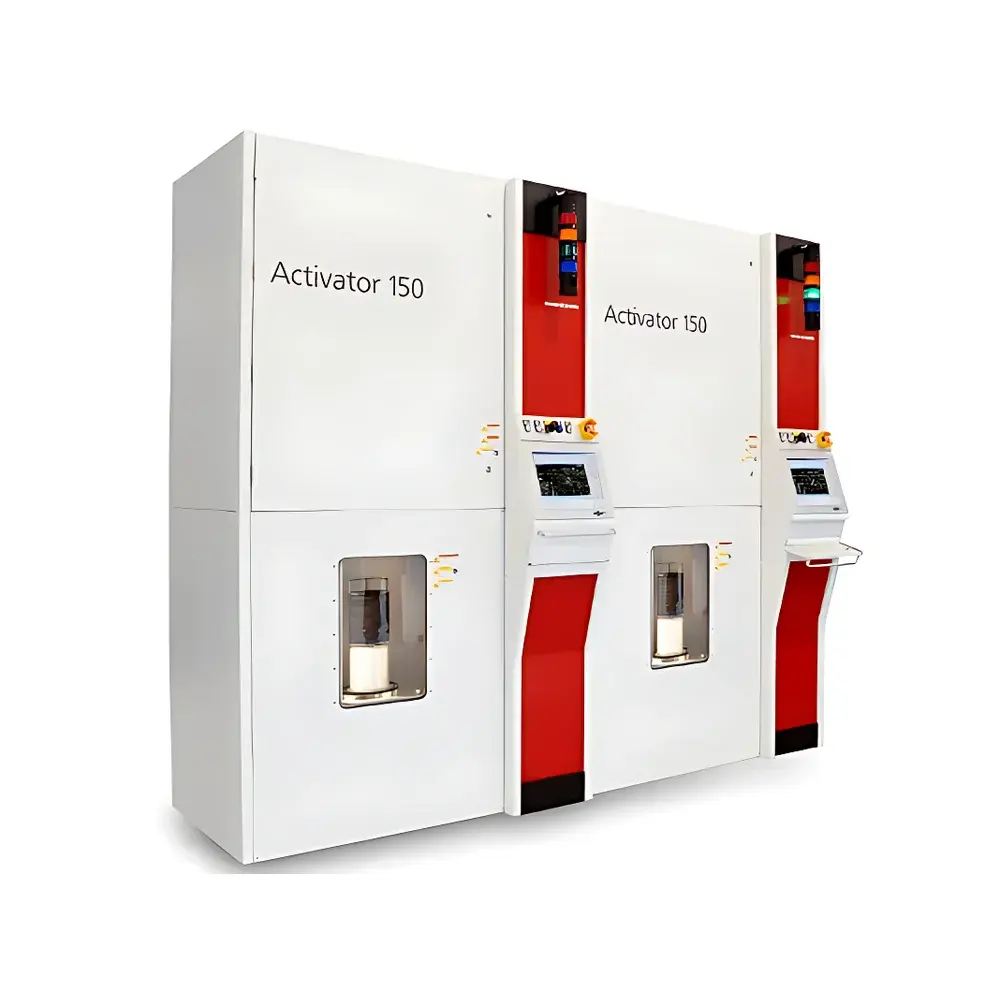
| Origin | Germany |
|---|---|
| Manufacturer Type | Authorized Distributor |
| Origin Category | Imported |
| Model | centrotherm Activator150 |
| Instrument Type | High-Vacuum Rapid Thermal Annealing Furnace |
| Sample Size | 150 mm (6-inch) wafers |
| Operating Atmosphere | Ambient pressure or controlled vacuum/pressure |
| Maximum Ramp Rate | 150 K/s |
| Maximum Cool-down Rate | 150 K/s |
| Temperature Accuracy | ±1 °C |
| Temperature Uniformity | ≥95% across wafer surface |
| Max Process Temperature | 1850 °C |
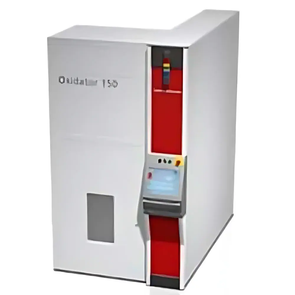
| Origin | Germany |
|---|---|
| Manufacturer Type | Authorized Distributor |
| Origin Category | Imported |
| Model | Centrotherm c.RAPID 150 / RTP 150 |
| Instrument Type | High-Vacuum Rapid Thermal Annealing Furnace |
| Sample Size | 6-inch wafer or substrate |
| Operating Atmosphere | Ambient pressure or controlled vacuum (1–50 mbar) |
| Max. Ramp Rate | 150 K/s |
| Max. Cool-down Rate | 150 K/s |
| Temperature Accuracy | ±1 °C |
| Temperature Uniformity | ±0.5 °C across 6″ wafer |
| Max. Process Temperature | 1150 °C (unlimited dwell at ≤750 °C) |
| Heating System | 24 independently PWM-controlled lamp arrays |
| Cooling Water Requirement | 20 L/min |
| Exhaust Flow | 250 m³/h |
| Substrate Compatibility | Si, GaAs, SiC, GaN, Sapphire, graphite carriers |
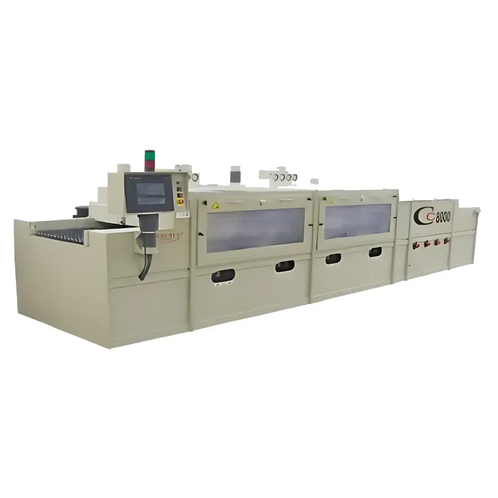
| Brand | Chemcut |
|---|---|
| Model | CC8000 |
| Origin | USA |
| Equipment Type | Horizontal Conveyor-Based Wet Processing System |
| Application Scope | Semiconductor Wafers (Cu, Ti/W etching), Leadframes (QFN/BGA), IC Substrates, HDI/FPC, Display Panels (LCD/Touch), Solar Cells, Precision Metal Parts |
| Spray Manifold Design | Optimized for Uniform Chemical Delivery & High-Resolution Pattern Transfer |
| Installed Base | >700 Systems Worldwide |
| Compliance Framework | Designed for GLP/GMP-aligned cleanroom integration and ASTM F2164-compliant wet process validation |
| Software Capability | PLC-based process control with recipe management, audit trail logging, and optional 21 CFR Part 11 compliance modules |
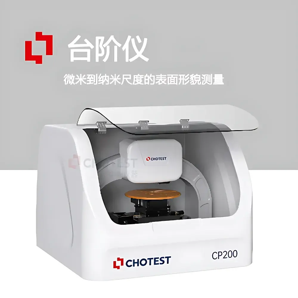
| Brand | Chotest |
|---|---|
| Origin | Guangdong, China |
| Manufacturer Type | Authorized Distributor |
| Country of Origin | China |
| Model | NS200 |
| Price | USD 84,000 (FOB Shenzhen) |
| Measurement Principle | Contact-mode stylus profilometry with LVDC capacitive transduction |
| Vertical Resolution | Sub-ångström (≤0.1 Å) |
| Lateral Scan Range | 55 mm |
| X/Y Stage Travel | 150 mm × 150 mm (motorized) |
| R-θ Stage | 360° continuous motorized rotation |
| Max Sample Thickness | 50 mm |
| Wafer Compatibility | 150 mm (6″) and 200 mm (8″) |
| Vertical Measurement Range | Up to 1000 µm |
| Force Control | 1–50 mg adjustable, electromagnetic micro-force actuation |
| Probe Tip Radius | 2 µm diamond |
| Optical Navigation | 5 MP color camera with real-time probe trajectory overlay |
| SPC Module | Integrated statistical process control with trend charts, Cp/Cpk, histogram, and outlier detection |
| Environmental Requirements | 16–25 °C (ΔT < 2 °C/h), 30–40% RH (non-condensing), floor vibration ≤ 6.35 µm/s (1–100 Hz), ambient noise ≤ 80 dB, laminar airflow ≤ 0.508 m/s downward |
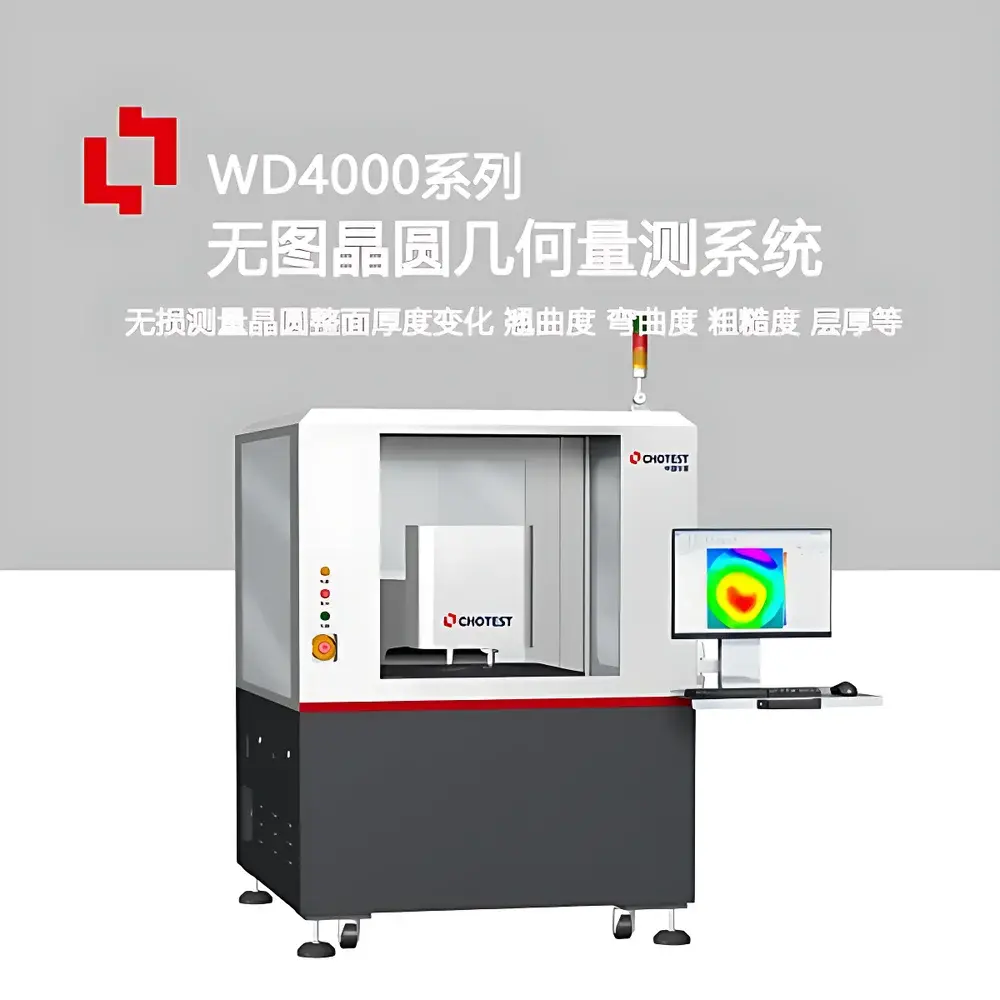
| Brand | Chotest |
|---|---|
| Origin | Guangdong, China |
| Manufacturer Type | Authorized Distributor |
| Country of Origin | China |
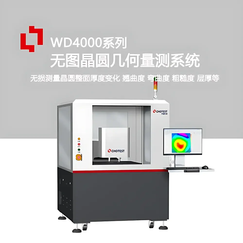
| Model | WD4000 |
| Price | USD 420,000 (FOB Shenzhen) |
| Thickness Range | 150 µm – 2000 µm |
| TTV/Bow/Warp Measurement Accuracy | ±0.1 µm (typical, calibrated per ISO 21287) |
| Z-Axis Resolution (Interferometry) | ≤ 0.1 nm |
| Lateral Scan Area | 400 mm × 400 mm |
| Vertical Travel | 75 mm |
| Maximum Wafer Size | 300 mm (12″) |
| Surface Reflectivity Range | 0.05% – 100% |
| Roughness RMS Repeatability | ≤ 0.005 nm (ISO 25178-6 compliant) |
| Interferometric Objective Options | 2.5×, 5×, 10×, 20×, 50× |
| Spectral Confocal Thickness Sensor | Dual-beam, high-stability SLED source, 90 µm measurement range (n = 1.5), minimum detectable thickness: 0.4 µm |
| Infrared Interferometry Module | SLED source, 37–1850 µm range |
| Scan Modes | Full-map, cross (‘X’), star (‘+’), user-defined multi-point |
| Compliance | ISO 5725 (accuracy & precision), ISO 25178-2 (areal texture), ISO 10110-7 (optical surface form), SEMI D39 (wafer geometry), ASTM F39 (silicon wafer bow/warp) |
| Brand | Chotest |
|---|---|
| Origin | Guangdong, China |
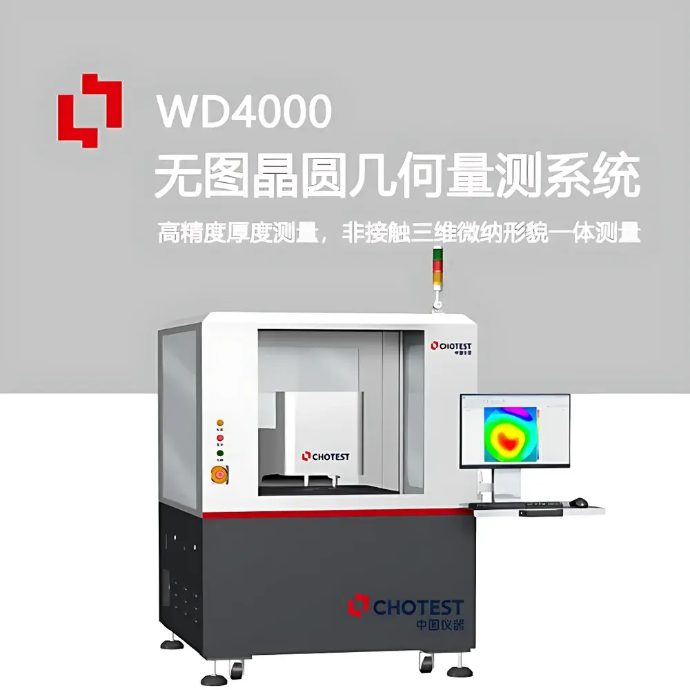
| Model | WD4000 |
| Thickness Range | 150 µm – 2000 µm |
| 3D Surface Topography Resolution (Z) | ≤ 0.1 nm |
| Roughness RMS Repeatability | ±0.005 nm |
| Supported Wafer Sizes | 4″, 6″, 8″, 12″ |
| Optical Principle | Spectral Confocal Dual-Side Scanning + White-Light Interferometry (WLI) |
| Max XY Travel | 400 mm × 400 mm |
| Z Travel | 75 mm |
| Scan Modes | Full-map, Cross (‘+’), Custom Multi-point |
| Interferometric Objective Options | 2.5×, 5×, 10×, 20×, 50× |
| Reflectivity Range | 0.05% – 100% |
| Film Thickness Range (IR Interferometry) | 37 µm – 1850 µm (n ≈ 1.5) |
| Minimum Detectable Film Thickness | 0.4 µm |
| Vacuum Chuck | ESD-Safe Perforated Ceramic Vacuum Stage |
| Brand | Chotest |
|---|---|
| Origin | Guangdong, China |
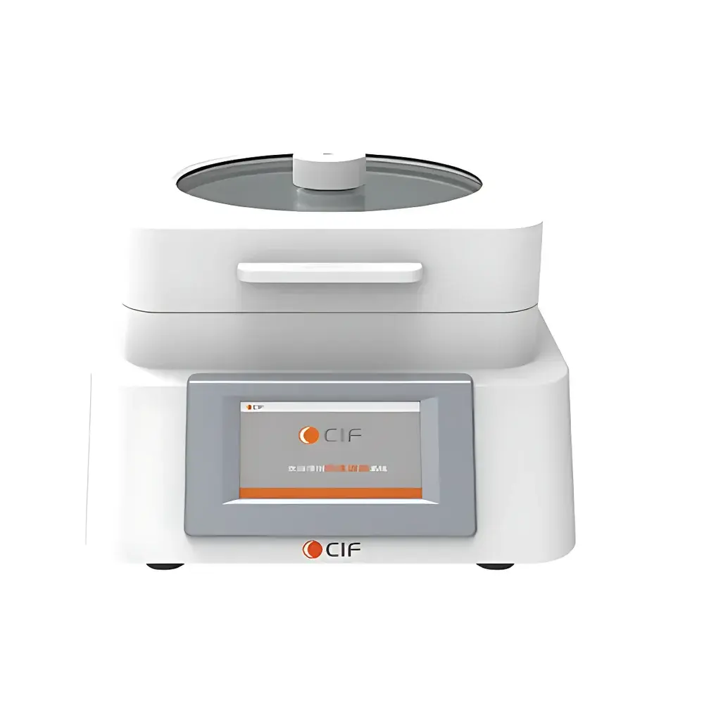
| Model | WD4000 |
| Measurement Principles | Spectral Confocal Reflectometry (thickness), White-Light Interferometry (3D topography) |
| Wafer Compatibility | 4″–12″ |
| Max. Scan Area | 400 mm × 400 mm |
| Z-Axis Resolution | ≤ 0.1 nm |
| Thickness Range | 150 µm – 2000 µm |
| Surface Reflectivity Range | 0.05% – 100% |
| Roughness RMS Repeatability | ±0.005 nm |
| Motion Stage | Granite-based龙门 with AC servo direct-drive & 0.1 µm encoder resolution |
| Environmental Isolation | Active vibration damping for sub-nm stability |
| Brand | CIF |
|---|---|
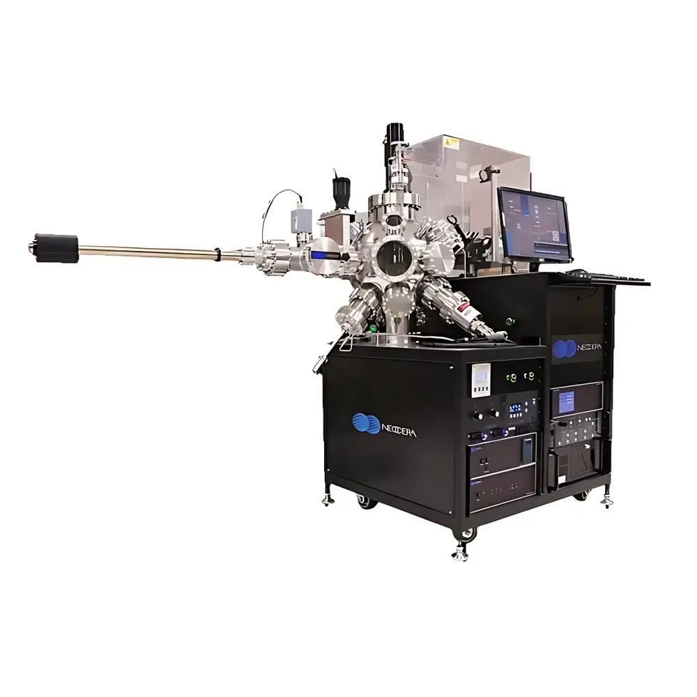
| Model | SC1 |
| Type | Benchtop Precision Spin Coater |
| Rotation Speed Range | 0–10,000 rpm |
| Speed Accuracy | ±1% |
| Acceleration Rate | 0–10,000 rpm/s |
| Substrate Compatibility | Ø150 mm (6-inch) wafers, square substrates up to 105 × 105 mm |
| Chamber Diameter | 180 mm |
| Drive System | Closed-loop servo motor with digital tachometric feedback |
| Control Interface | 7-inch full-color capacitive touchscreen (bilingual English/Chinese) |
| Programmability | Standard 10-step gradient program |
| Safety | Dual interlocked lid with electromagnetic cut-off, PTFE-embedded tempered glass upper chamber, vacuum-sealed chuck interface, triple-seal sample tray mounting |
| Construction | Powder-coated stainless steel housing |
| Chamber Lining | PTFE |
| Chuck Material | NPP-H polypropylene (acid/alkali resistant) |
| Optional Accessories | N₂ purge kit, N₂ inert atmosphere module, automated dispense system, manual dropper kit |
| Compliance | Designed for ISO Class 5–7 cleanroom integration |
| Brand | Neocera |
|---|---|
| Origin | USA |
| Model | Combinatorial PLD System |
| System Type | Turnkey Pulsed Laser Deposition Platform with Continuous Composition Spread (CCS-PLD) Capability |
| Substrate Compatibility | 2-inch wafers (4-inch and 6-inch available on request) |
| Operating Environment | Up to 800 °C, up to 500 mTorr O₂ partial pressure |
| Deposition Mode | Standard PLD + CCS-PLD (Continuous Composition Spread) |
| Target Configuration | Multi-target carousel for binary/ternary/quaternary combinatorial synthesis |
| Film Architecture Support | Epitaxial thin films, multilayer heterostructures, superlattices |
| Oxygen Compatibility | Fully compatible with reactive oxygen ambient for metal oxide epitaxy |
| Post-deposition Annealing | Not required due to in-situ compositional grading and kinetic control |
| Maskless Operation | Enabled by angular deposition gradient and laser fluence modulation |
| Layer Resolution | Sub-monolayer precision per pulse cycle |
| Compliance | Designed for GLP-compliant thin-film R&D environments |
| Brand | MicroChem Corp |
|---|---|
| Origin | USA |
| Model | MMA(8.5)MAA |
| Solvent System | Ethyl Lactate |
| Viscosity Range | Adjustable via Concentration (Typical Spin-Coated Film Thickness: 50–500 nm) |
| Packaging Options | 500 mL, 1 L, 4 L, 20 L HDPE Bottles |
| Recommended Storage | 10–27 °C |
| Developer | MIBK:IPA (1:3 v/v) |
| Stripper | Remover PG |
| Diluent | A Thinner |
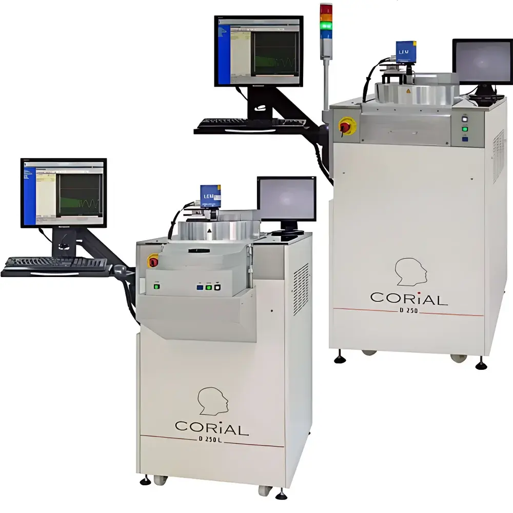
| Brand | Corial |
|---|---|
| Origin | France |
| Model | D250L |
| Heating Method | Hot-Wall |
| Deposition Rate | 520 nm/min |
| Process Gases | SiH₄, NH₃, N₂ |
| Deposited Films | SiO₂, Si₃N₄, SiOF, SiOCH, SiC |
| Base Vacuum | −300 to 50 mTorr |
| Operating Pressure | 0.2–2 Torr |
| Maximum Substrate Size | 200 mm (8-inch) wafers |
| Configuration | Load-Lock with Turbo-Molecular Pump (350 L/s) and Dry Scroll Pump (110 m³/h) |
| RF Power Supply | 300 W, 13.56 MHz |
| Integrated Controllers | TMP, Heater, HV/LV, Plasma Process Controller |
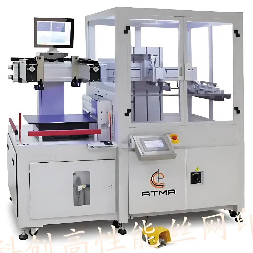
| Brand | Coruna |
|---|---|
| Origin | Jiangsu, China |
| Manufacturer Type | Authorized Distributor |
| Regional Category | Domestic (PRC) |
| Model | Screen Printer |
| Price | USD 1.00 (FOB Jiangsu, Ex-Works) |
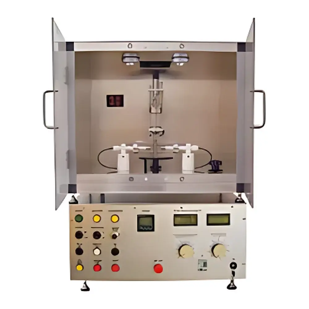
| Brand | Kaige |
|---|---|
| Origin | Germany |
| Model | CTI-4 |
| Test Voltage Range | Up to 600 V |
| Droplet Volume | Standardized per IEC 60112 (0.1% NH₄Cl solution) |
| Droplet Height | 35 mm |
| Electrode Dimensions | 2 mm × 5 mm Pt |
| Timing Interval | 30 s per droplet |
| Compliance | IEC 60112:2003, UL 746A, ASTM D3638-92, DIN EN 60112, VDE 0303-1 |
| Automation Level | Fully Automated |
| Measurement Outputs | CTI (Comparative Tracking Index), PTI (Proof Tracking Index) |
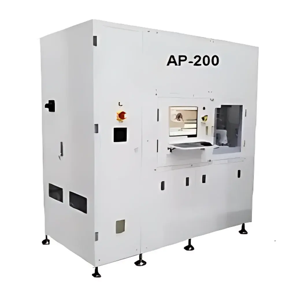
| Brand | CTS |
|---|---|
| Origin | South Korea |
| Model | AP200 |
| Wafer Size Compatibility | 4", 6", 8" |
| Platen Count | 1 |
| Platen Speed | 0–200 rpm |
| Polishing Head Speed | 0–200 rpm |
| Polishing Head Oscillation Range | ±15 mm |
| Pressure Control Zones | 3 (Center, Edge, Retaining Ring) |
| Pressure Range | 0.14–14 psi |
| Platen Diameter | 20 in |
| Slurry Flow Rate | 20–500 cc/min (via dual peristaltic pumps) |
| Conditioning Head | 10-zone segmented actuation |
| Conditioning Sweep Speed | 10 sweeps/min |
| Conditioning Downforce | 3–20 lbs |
| Conditioning Speed | 0–150 rpm |
| Within-Wafer Non-Uniformity (WIWNU, 5-mm edge exclusion) | <5% (1σ) |
| Wafer-to-Wafer Non-Uniformity (WTWNU, 5-mm edge exclusion) | <3% (1σ) |
| Dimensions (W×L×H) | 1000 × 2030 × 2100 mm |
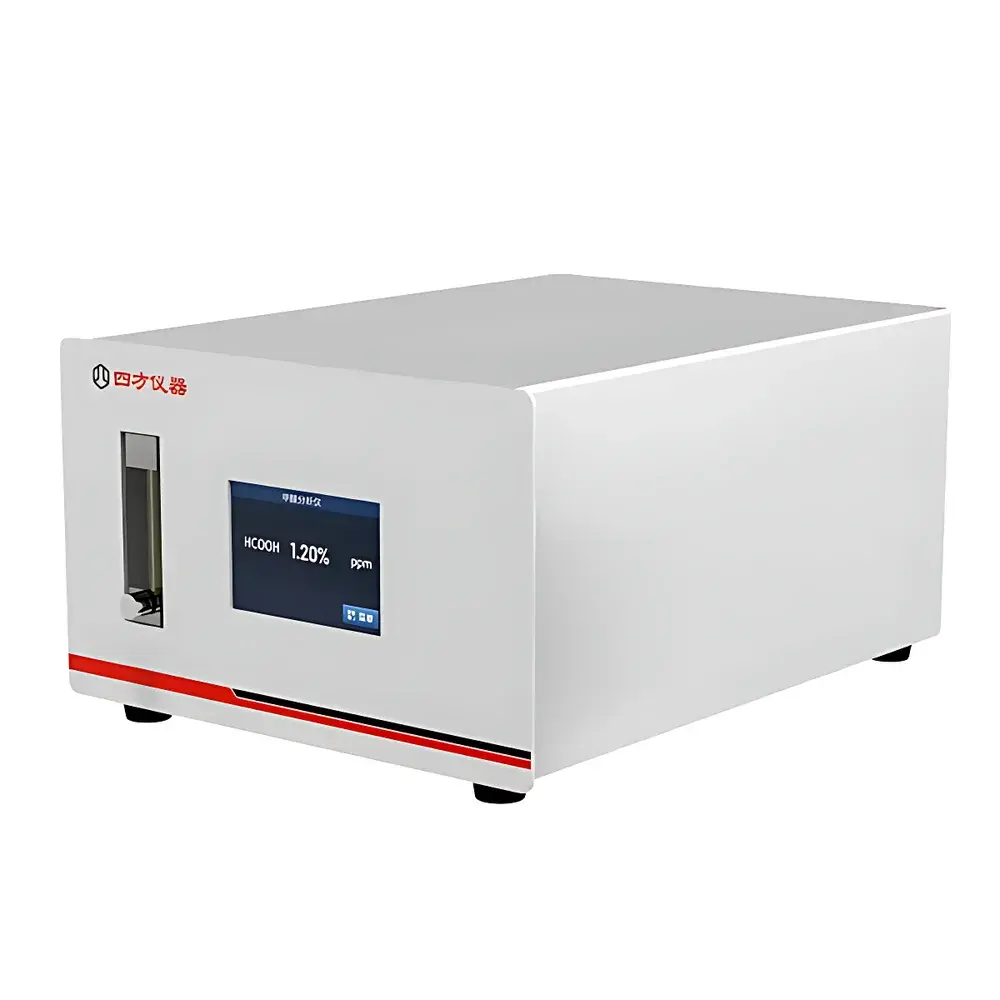
| Brand | CUBIC INSTRUMENTS |
|---|---|
| Origin | Hubei, China |
| Manufacturer Type | Authorized Distributor |
| Regional Category | Domestic (PRC) |
| Model | Not Specified |
| Pricing | Upon Request |
| Measurement Principle | Non-Dispersive Infrared (NDIR) |
| Range Options | 0–5% v/v, 0–10% v/v, 0–30% v/v |
| Accuracy | ≤ ±2% FS |
| Repeatability | ≤ ±1% FS |
| Response Time (T90) | ≤ 60 s |
| Operating Temperature | 0–50 °C |
| Relative Humidity | 0–95% RH (non-condensing) |
| Communication Interfaces | RS-232, RS-485 |
| Power Supply | 24 VDC or 100–240 VAC |
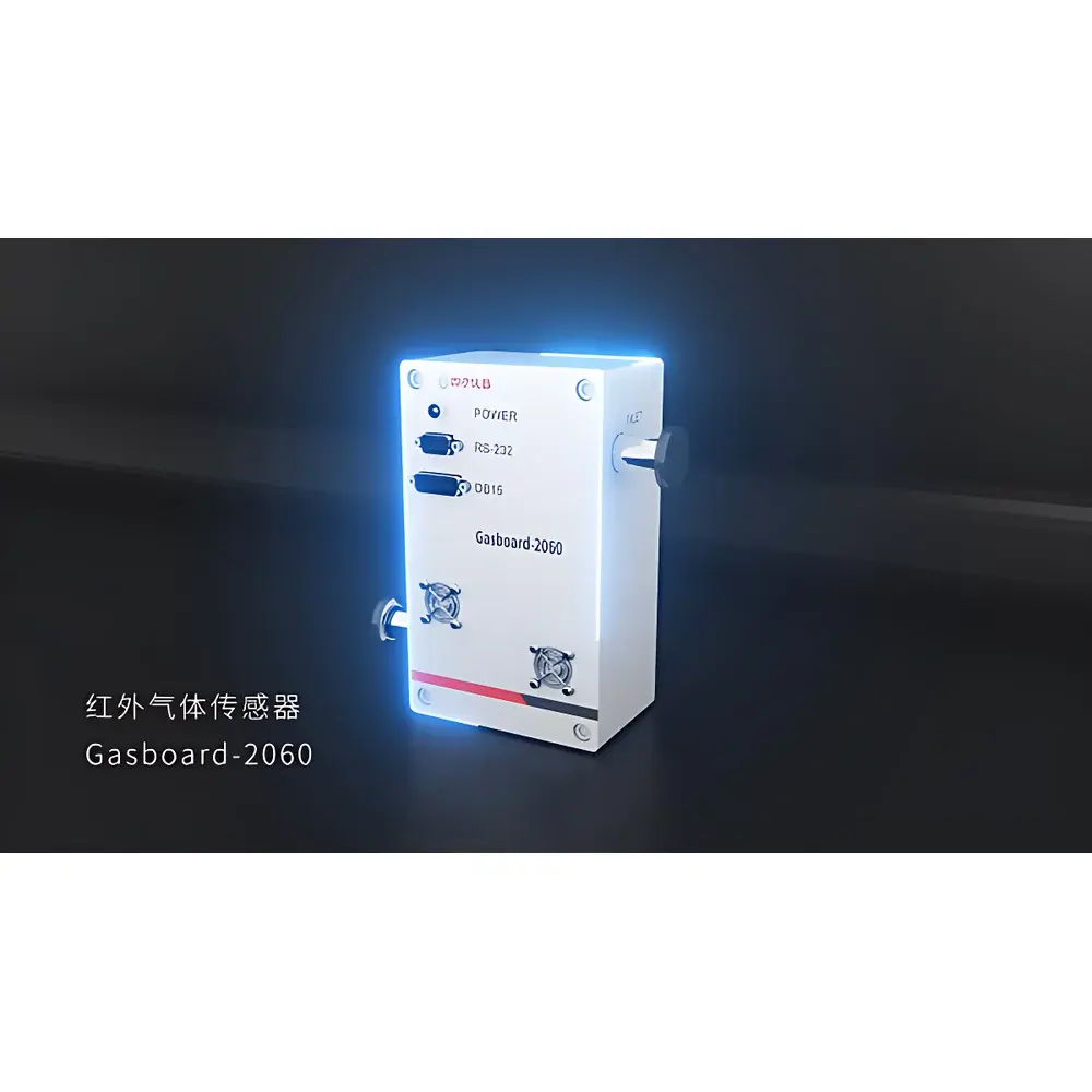
| Brand | CUBIC INSTRUMENTS |
|---|---|
| Origin | Hubei, China |
| Model | Gasboard-2060 |
| Detection Principle | Non-Dispersive Infrared (NDIR) |
| Target Gases | SiF₄, CF₄, SF₆, NF₃, CO₂ |
| Range | 1–264 ppm (0–200 mTorr) |
| Repeatability | ±0.5% of reading |
| Linearity | ±1% F.S. |
| Detection Limit | 1 ppm |
| Output | Analog (4–20 mA) and Digital (RS485/Modbus RTU) |
| Housing | 316L stainless steel, CF-40 flange compatible |
| Operating Temperature | 0–50 °C |
| Pressure Rating | ≤200 mTorr (vacuum-compatible) |
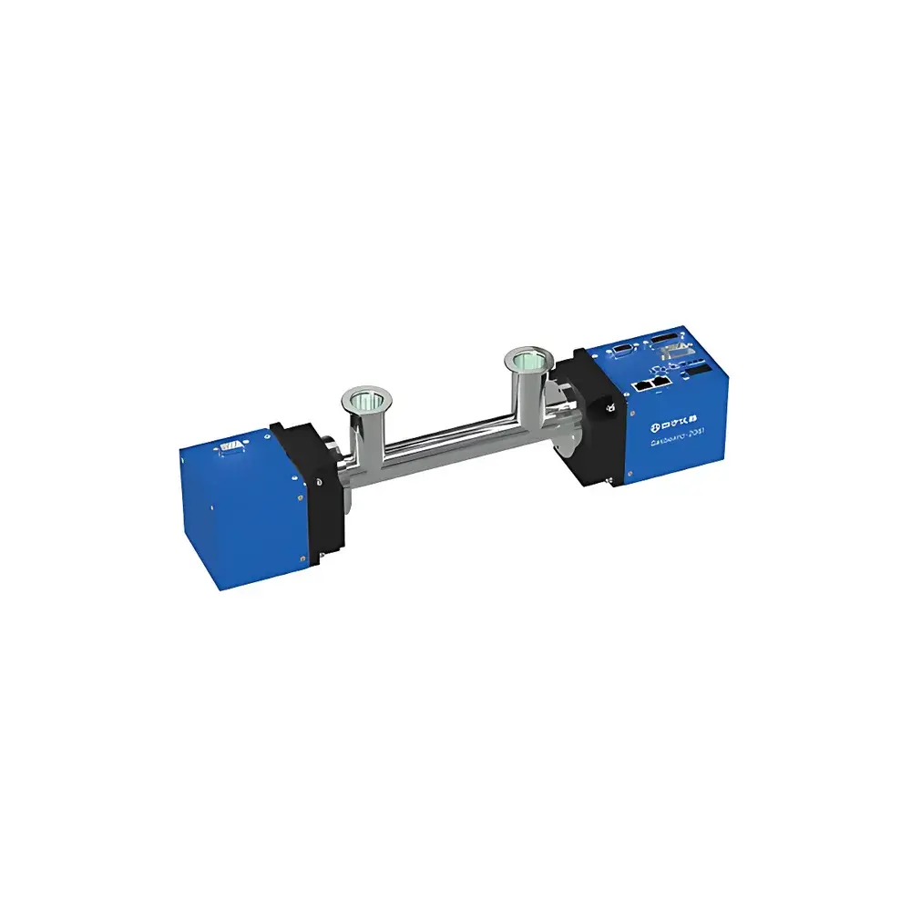
| Brand | CUBIC INSTRUMENTS |
|---|---|
| Origin | Hubei, China |
| Model | Gasboard-2061 |
| Detection Principle | Non-Dispersive Infrared (NDIR) |
| Target Gases | WF₆, CF₄, SF₆, NF₃, CO₂ |
| Measurement Range | 1–264 ppm (0–200 mTorr) |
| Repeatability | ±0.5% |
| Linearity | ±1% F.S. |
| Detection Limit | 1 ppm |
| Output Interface | Analog (4–20 mA) and Digital (RS485/Modbus RTU) |
| Housing Material | 316L Stainless Steel |
| Process Connection | CF-35 or ISO-KF40 Flange Compatible |
| Operating Temperature | 0–50 °C |
| Pressure Rating | Up to 200 mTorr (absolute) |
| Brand | CUBIC INSTRUMENTS |
|---|---|
| Origin | Hubei, China |
| Manufacturer Type | Authorized Distributor |
| Country of Origin | China |
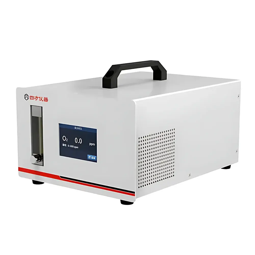
| Model | Gasboard-3053 |
| Measurement Range | 0–10 / 0–100 / 0–1000 ppm & 0–25% O₂ (auto-ranging) |
| LOD | 0.5 ppm |
| Resolution | 0.1 ppm |
| Accuracy | ≤±2% F.S. or ±0.5 ppm (whichever is greater) |
| T90 Response Time | ≤10 s |
| Warm-up Time | ≤20 min |
| Zero Drift | ±0.5% F.S. |
| Span Drift | ±0.5% F.S. |
| Repeatability | ±0.5% F.S. |
| Sampling Flow | 0.5–1 L/min |
| Communication | RS-232, RS-485 |
| Gas Interface | 1/4″ VCR-F (inlet & outlet) |
| Dimensions (L×W×D) | 210×134×300 mm |
| Operating Temp. | 0–50 °C |
| Humidity | 0–95% RH (non-condensing) |
| Brand | Cyberstar |
|---|---|
| Origin | France |
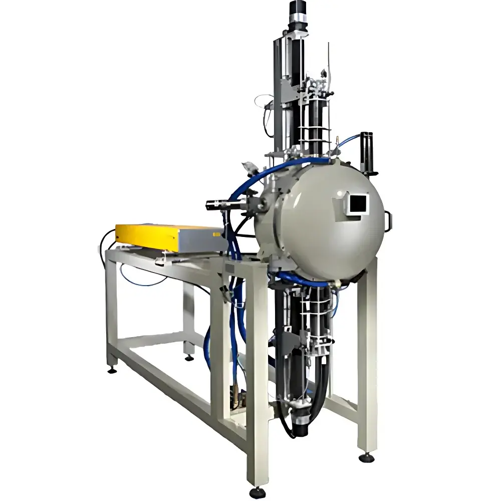
| Model | LHPG |
| Heating Source | High-Power Diode or CO₂ Lasers |
| Max Temperature | >2800 °C |
| Pulling Stroke | 140 mm |
| Pulling & Rotation Speeds | Precisely Adjustable |
| Atmosphere Control | High-Purity Ar, O₂, N₂, H₂, or Mixed Gases |
| Pressure Range | Up to 1.5 bar (abs) |
| Vacuum Level | ≤1×10⁻⁴ mbar |
| In Situ Monitoring | Real-Time CCD Imaging + Non-Contact Infrared Pyrometry |
| Crystal Geometry | Single-Crystal Fibers (Typical Ø 0.3–2.0 mm) |
| Crucible-Free Operation | Yes |
| Applicable Materials | Refractory Oxides (e.g., SrTiO₃), Nitrides, Carbides, and Other High-Melting-Point Compounds |