
Other Semiconductor Inspection Instruments
Filter
Showing 121–150 of 217 results
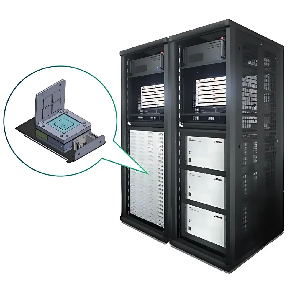
| Brand | McScience |
|---|---|
| Origin | South Korea |
| Manufacturer Type | Authorized Distributor |
| Origin Category | Imported |
| Model | M6000 UVX |
| Pricing | Upon Request |
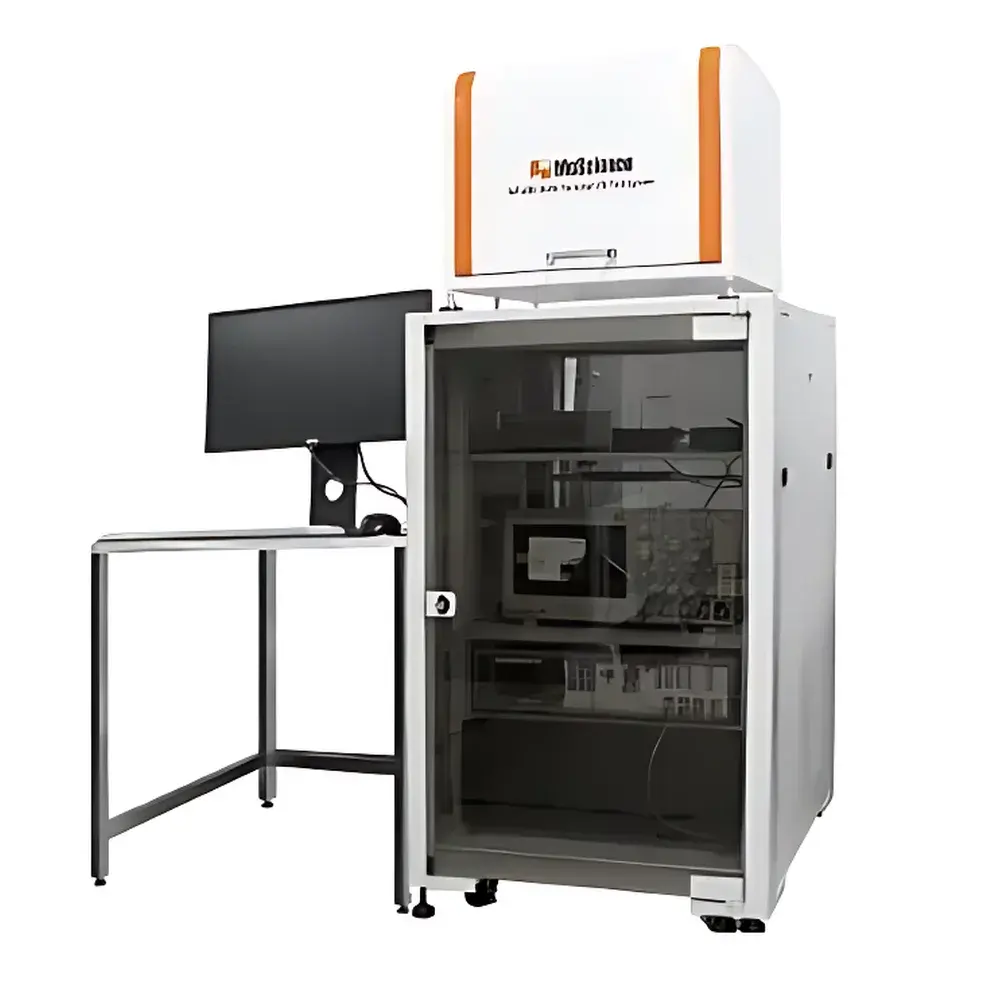
| Brand | McScience |
|---|---|
| Origin | South Korea |
| Model | M6200 |
| Application | Transient EL/PL, Carrier Dynamics, Low-Temperature Spectroscopy |
| Excitation Sources | Precision Current Pulse Generator (for Tr-EL) & Ultrafast Pulsed Laser (for TR-PL) |
| Temperature Range | 10 K – 300 K (with Closed-Cycle Cryostat) |
| Detection | Time-Correlated Single Photon Counting (TCSPC) or Fast Digitizer (up to 1 GS/s) |
| Spectral Resolution | < 0.5 nm (with 1/4 m Monochromator) |
| Temporal Resolution | < 50 ps (TR-PL), < 100 ns (Tr-EL) |
| Compliance | ASTM F2891–22 (OLED Device Testing), ISO/IEC 17025–2017 (Calibration Traceability) |
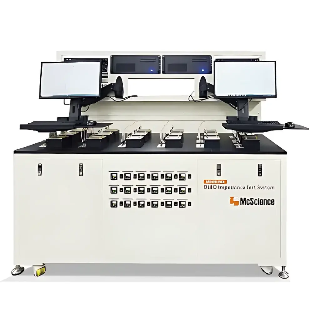
| Brand | McScience |
|---|---|
| Origin | South Korea |
| Manufacturer Type | Authorized Distributor |
| Origin Category | Imported |
| Model | M6400 |
| Pricing | Upon Request |
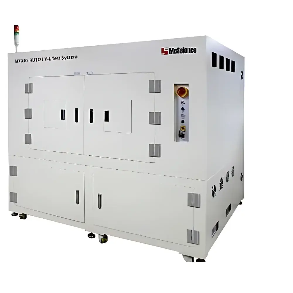
| Brand | McScience |
|---|---|
| Origin | South Korea |
| Model | M7000 |
| Category | Imported Semiconductor Inspection Instrument |
| Configuration | Multi-Channel I-V-L & Degradation Monitoring Platform |
| Optical Detection | Integrated Spectrometer and Tristimulus Colorimeter with Motorized XYZ Positioning |
| Thermal Control | Independent Temperature Chamber (−40 °C to +120 °C) |
| Electrical Biasing | Precision Source-Measure Units (SMUs) for DC/Pulsed Operation |
| Measurement Modes | Luminance (cd/m²), Chromaticity (CIE 1931 xy), Spectral Power Distribution (380–780 nm), EQE, Impedance (1 Hz–1 MHz), Viewing Angle (±85°), Transient EL (µs–s resolution) |
| Compliance | ASTM F2699, ISO 13406-2, IEC 62341-6-1, JEDEC JESD22-A108 (HTOL), USP <1058> (Analytical Instrument Qualification) |
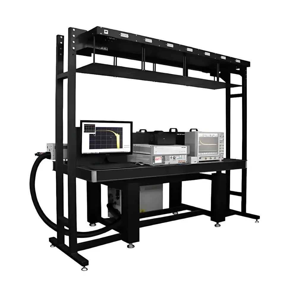
| Brand | McScience |
|---|---|
| Origin | South Korea |
| Model | T3000 PLUS |
| Application | Transient charge dynamics characterization of organic optoelectronic devices |
| Core Excitation Source | Nanosecond-pulsed laser system |
| Timing Resolution | Sub-nanosecond delay control |
| Bias Control | Programmable DC/AC voltage source (±100 V, <10 mV resolution) |
| Detection Bandwidth | DC to 2 GHz (current amplification + digitization) |
| Compliance | Fully compatible with ISO/IEC 17025 laboratory practices for transient electrical measurements |
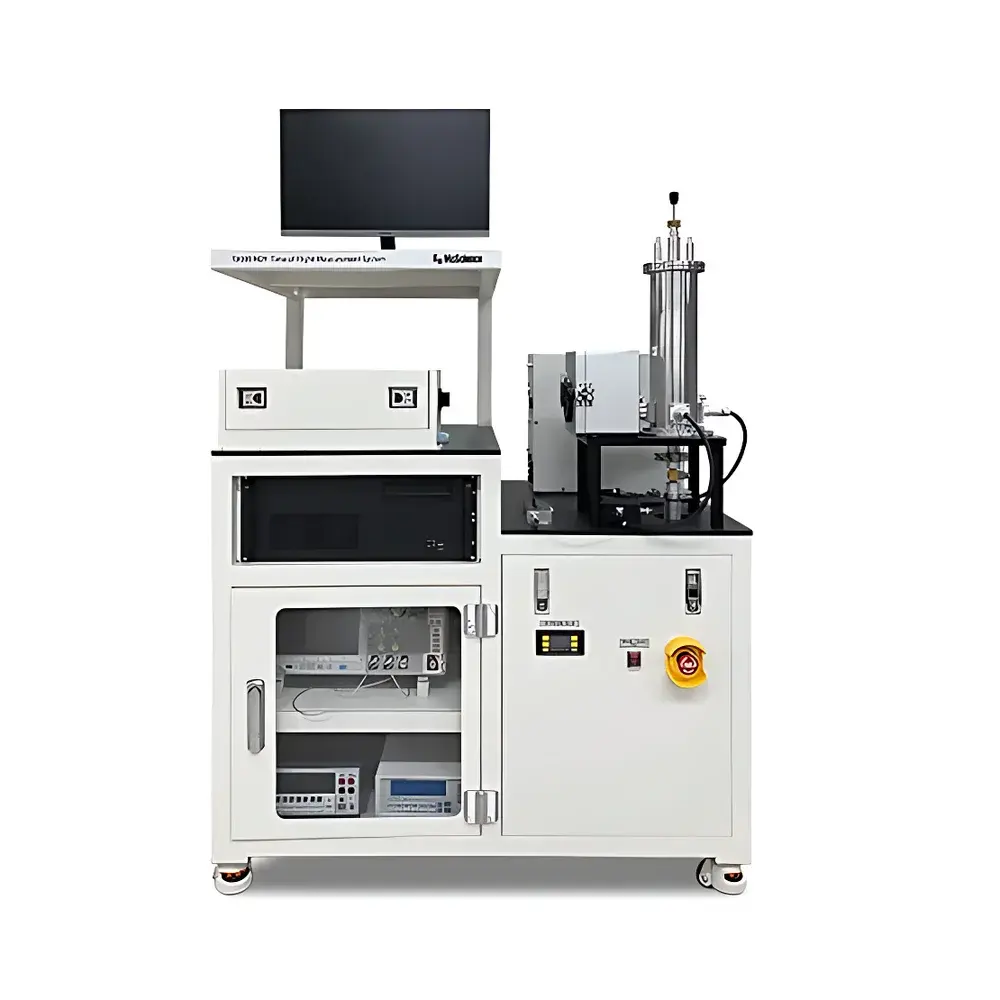
| Brand | McScience |
|---|---|
| Origin | South Korea |
| Model | T3000 |
| Type | Time-of-Flight Carrier Mobility Characterization System |
| Application Domain | Organic Light-Emitting Diode (OLED) Materials & Thin-Film Semiconductor Research |
| Temperature Range | 10 K to 350 K (with optional cryostat integration) |
| Excitation Source | Pulsed UV–Vis Laser (e.g., 355 nm or 405 nm, <10 ns pulse width) |
| Detection Bandwidth | ≥500 MHz transient current acquisition |
| Measurement Modes | Standard TOF, Dark Injection Transient (DIT), Charge Extraction by Linearly Increasing Voltage (CELIV) |
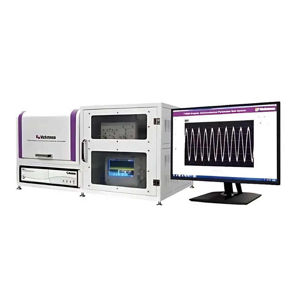
| Brand | McScience |
|---|---|
| Origin | South Korea |
| Model | T4000 |
| Type | Integrated Organic Semiconductor Parameter Measurement System |
| Light Source | High-Stability LED Array |
| Measurement Modes | TPV, TPC, Linear Ramp Charge Extraction (Dark & Photo), Transient Electroluminescence, DC I–V, Impedance Spectroscopy (IS), Capacitance–Voltage (C–V), IMVS, IMPS |
| Compliance | Designed for ISO/IEC 17025-aligned laboratory environments |
| Software Interface | Windows-based with automated script execution and raw data export (CSV, TXT, HDF5) |
| Data Acquisition | 16-bit ADC, up to 1 MS/s sampling rate |
| Voltage Range | ±20 V (programmable), Current Range: ±100 mA (auto-ranging) |
| Environmental Operation | 15–35 °C, <70% RH non-condensing |
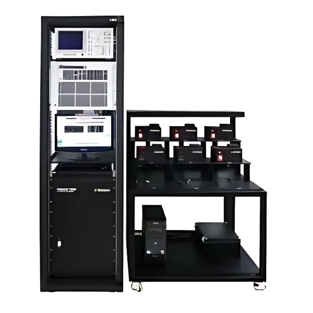
| Brand | McScience |
|---|---|
| Origin | South Korea |
| Model | T5000 |
| Channel Configuration | Single-Channel & Multi-Channel |
| Test Modes | Standard, Thermal Stress, Photo-Stress |
| Measurement Capabilities | Field-Effect Mobility (µFE), Saturation Mobility (µSAT), On/Off Current Ratio (Ion/Ioff), Threshold Voltage (Vth), Subthreshold Swing (SS) |
| Compliance | Designed for semiconductor device characterization per JEDEC JESD22-A108 (reliability), ISO/IEC 17025-compliant test environments |
| Software | McTestSuite v4.2 with GLP/GMP audit trail support |
| Brand | McScience |
|---|---|
| Origin | South Korea |
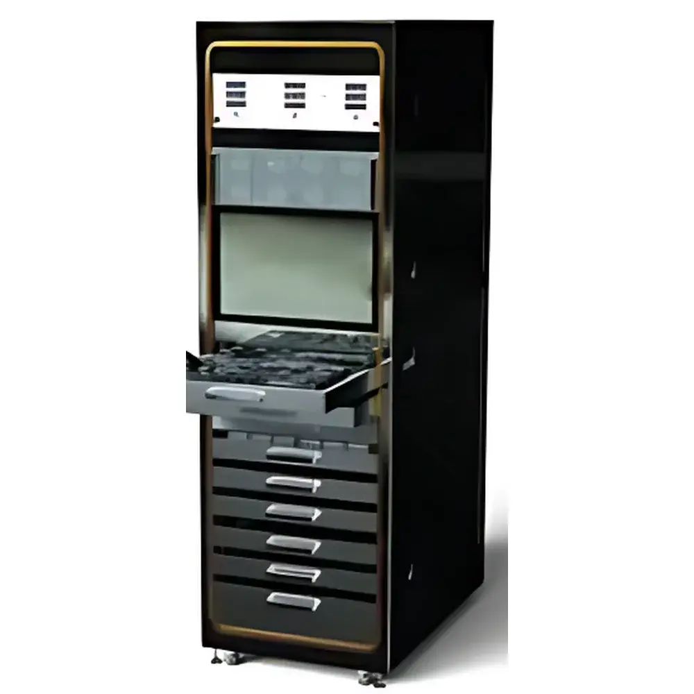
| Model | T6000 |
| Detection Principle | Calcium Thin-Film Degradation Assay |
| Temperature Range | 15–85 °C (±0.1 °C stability) |
| Humidity Range | 5–90 % RH (±1 % RH accuracy) |
| WVTR Measurement Range | 1×10⁻⁶ – 1×10⁻¹ g/m²/day |
| Channel Capacity | Up to 8 independent test channels |
| Electrical Measurement | DC resistance/conductance with ±0.05 % reading accuracy |
| Environmental Chamber | Dual-zone, programmable ramping profiles |
| Compliance | ASTM F1249, ISO 15106-3, JIS K 7129 |
| Brand | MicroChem Corp |
|---|---|
| Origin | Guangdong, China |
| Manufacturer Type | Authorized Distributor |
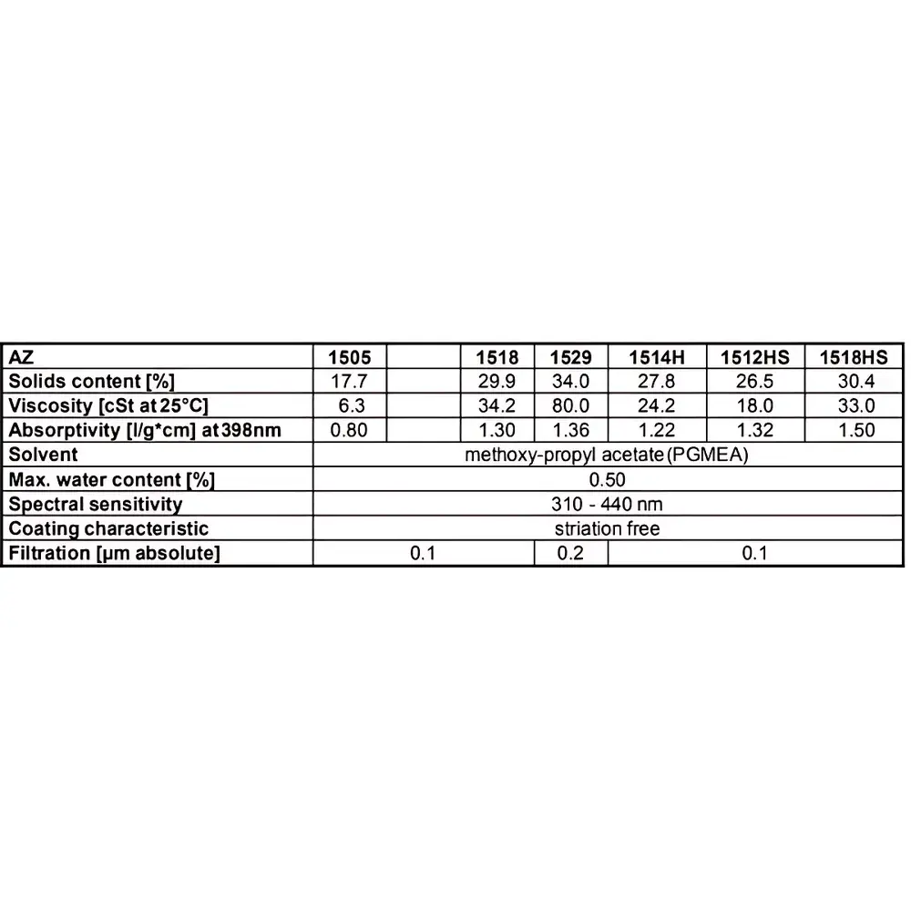
| Product Line | AZ1500 Series |
| Solvent System | Propylene Glycol Monomethyl Ether Acetate (PGMEA) |
| UV Sensitivity Range | 310–440 nm (i-, h-, g-line) |
| Recommended Development Time | AZ1500/AZ1514H: 50–60 s |
| AZ1500HS | 20–30 s |
| Compatible Developers | AZ 351B (1:4 dilution), 0.5% NaOH, AZ 726MIF |
| Film Thickness Range | 0.5–4.0 μm (spin-coated) |
| Storage Conditions | 0–25°C, sealed container, light-protected |
| Shelf Life | Batch-specific (see label: YYYY/MM/DD) |
| Compliance | Fully compatible with standard semiconductor cleanroom protocols and ISO Class 5–7 environments |
| Brand | MicroChem Corp |
|---|---|
| Origin | USA |
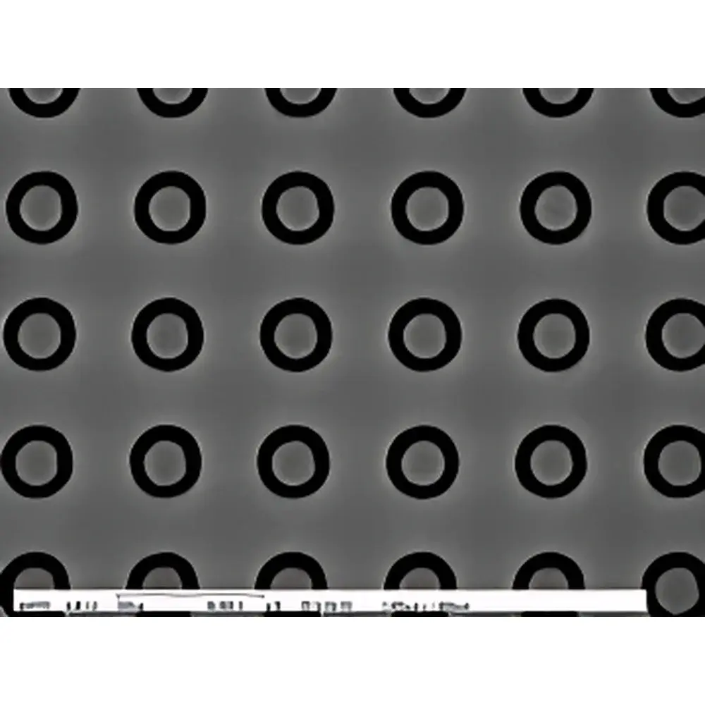
| Product Variants | gL2000-L, gL2000-M, gL2000-H |
| Developer Options | gL Developer, gL Developer HR |
| Rinse Agent | gL Rinse |
| Stripper | gL Remover |
| Etch Resistance | Superior to PMMA |
| Resolution Capability | Sub-10 nm (under optimized e-beam conditions) |
| Tone | Negative |
| Processing | Aqueous-based development |
| Brand | MicroChem Corp |
|---|---|
| Origin | USA |
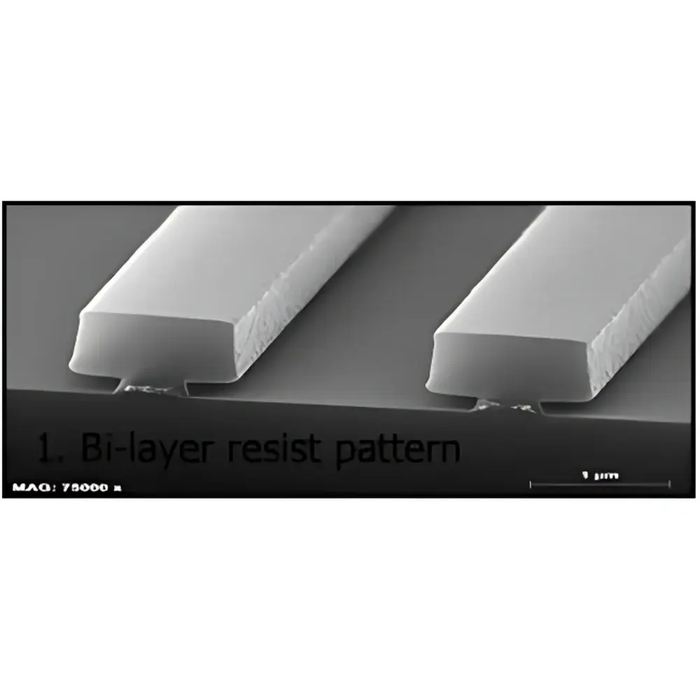
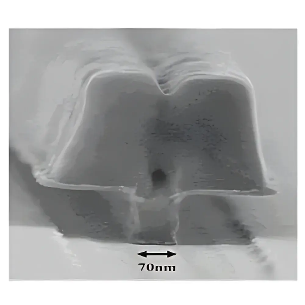
| Model | PMGI/LOR |
| Type | Negative Tone Bilayer Lift-Off Resist |
| Thermal Glass Transition (Tg) | ~190 °C |
| Resolution Capability | ≤ 0.25 µm |
| Maximum Compatible Metal Thickness | > 3 µm |
| Developer | MicroChem 101 Developer |
| Stripper | MicroChem Remover PG |
| Diluent | MicroChem G Thinner |
| Recommended Storage Temperature | 4–27 °C |
| Process Ambient | 20–25 °C ±1 °C, 35–45% RH ±2% |
| Brand | MicroChem |
|---|---|
| Origin | USA |
| Model | PMMA Series (495A, 495C, 950A, 950C) |
| Solvent Options | Anisole (A-series) or Chlorobenzene (C-series) |
| Resolution Capability | <100 nm |
| Recommended Developer | MIBK:IPA (1:3 v/v) |
| Stripper | Remover PG |
| Diluent | A Thinner |
| Storage Temperature | 10–27 °C |
| Compliance | Compatible with standard e-beam lithography workflows per ASTM E1981 and ISO/IEC 17025-accredited lab practices |
| Brand | MicroChem Corp |
|---|---|
| Origin | USA |
| Product Type | Inkjet-Compatible Negative Tone Photoresist |
| Model | PriElex® SU-8 1.0 |
| Curing Temperature | <150 °C |
| Optical Transparency | High (UV–Visible Range) |
| Chemical Resistance | Excellent (against common acids, bases, and solvents) |
| Young’s Modulus | Low (~2–4 GPa, typical for flexible SU-8 derivatives) |
| Layer Compatibility | Single- and multi-layer stackable |
| Developer Compatibility | Standard SU-8 aqueous alkaline developers (e.g., Microposit®显影液 equivalents) |
| Printer Compatibility | Fujifilm Dimatix DMP-series inkjet platforms (e.g., DMP-2831, DMP-3000) |
| Brand | Zhengye |
|---|---|
| Origin | Guangdong, China |
| Manufacturer Type | OEM Manufacturer |
| Origin Category | Domestic (China) |
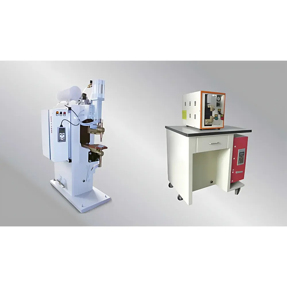
| Model | PY Series |
| Pricing | Available Upon Request |
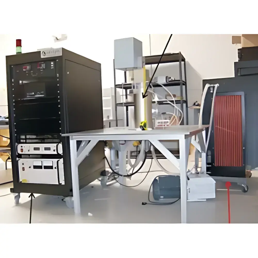
| Origin | USA |
|---|---|
| Manufacturer Type | Authorized Distributor |
| Origin Category | Imported |
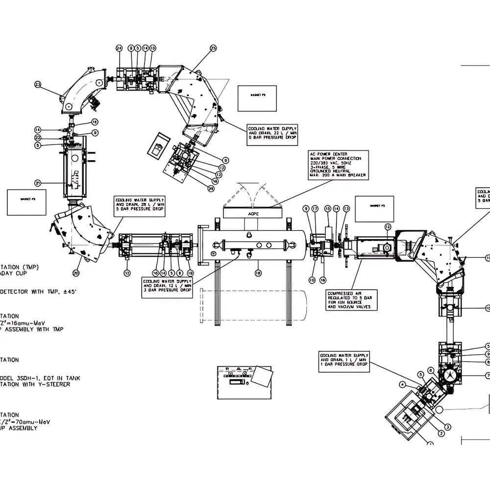
| Model | NEC UAMS |
| Price | USD $5,000,000 |
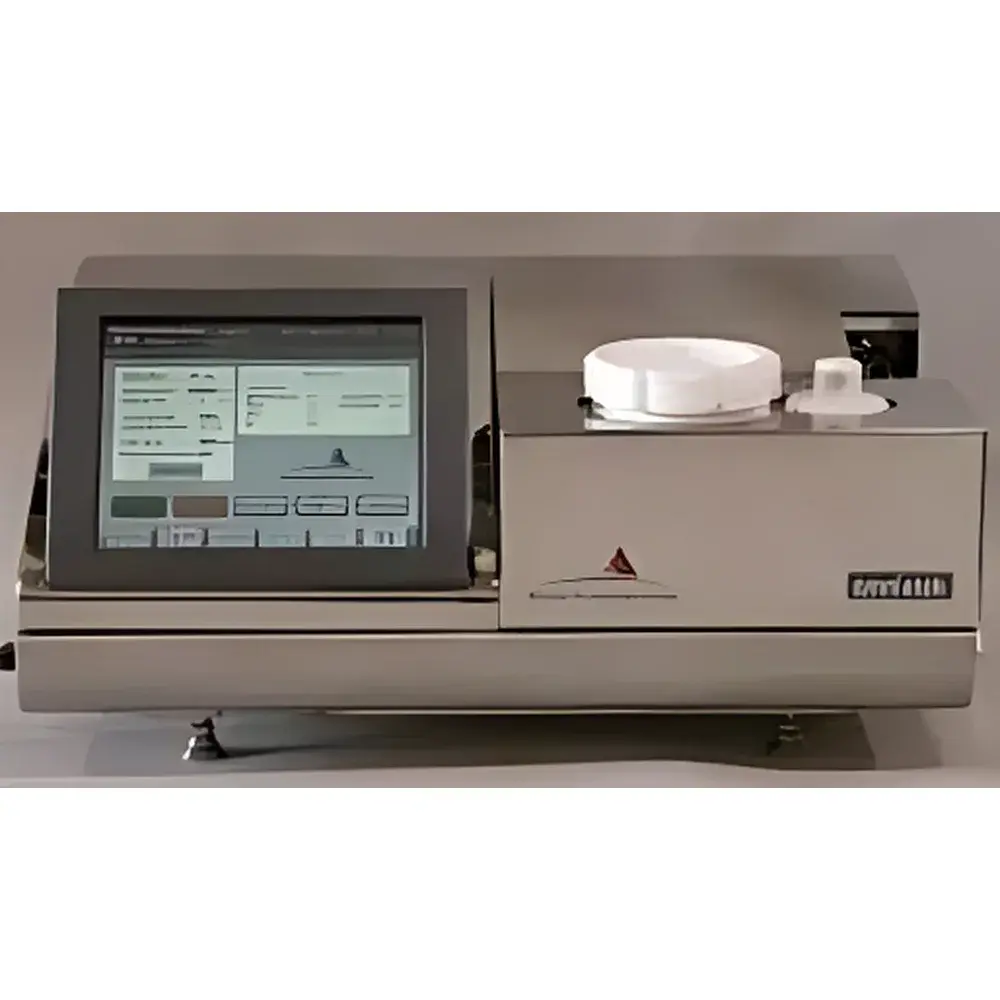
| Origin | USA |
|---|---|
| Manufacturer Type | Distributor |
| Origin Category | Imported |
| Model | DD110M110 |
| Pricing | Upon Request |
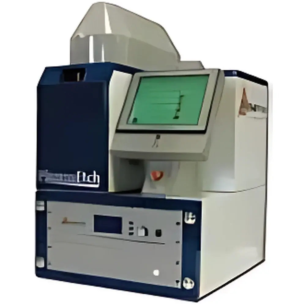
| Brand | Nisene |
|---|---|
| Origin | USA |
| Manufacturer Type | Authorized Distributor |
| Product Category | Imported |
| Model | OmniEtch |
| Pricing | Available Upon Request |
| Brand | Nisene |
|---|---|
| Origin | USA |
| Manufacturer Type | Authorized Distributor |
| Origin Category | Imported |
| Model | PlasmaEtch |
| Pricing | Available Upon Request |
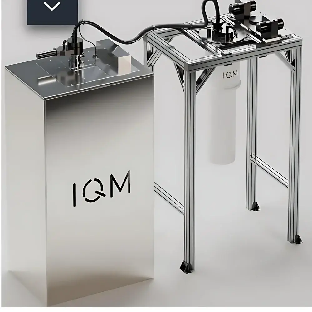
| Brand | 1124123/13213112 |
|---|---|
| Origin | France |
| Supplier Type | Authorized Distributor |
| Import Status | Imported |
| Model | NISQ-5 |
| Price | USD 1.4M (FOB) |
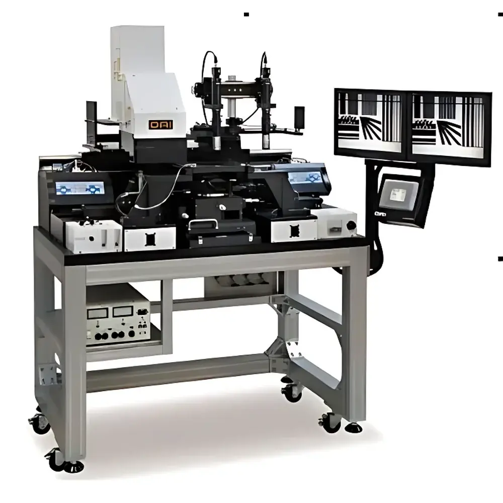
| Brand | OAI |
|---|---|
| Origin | USA |
| Model | MODEL 800MBA |
| Exposure Modes | Proximity, Soft Contact, Hard Contact, Vacuum Contact |
| Maximum Mask Size | 9" × 9" (228.6 mm × 228.6 mm) |
| Maximum Wafer Size | 200 mm (8-inch) |
| Light Source Type | High-Uniformity Broadband UV Lamp System |
| Alignment Accuracy | ≤ ±0.5 µm (typical, with optional auto-alignment upgrade) |
| Baseplate Thermal Stability | < ±0.1 °C over 4 hours |
| Compliance | ASTM F39–22 (Photolithography Equipment), ISO 14644–1 Class 5 Cleanroom Compatible |
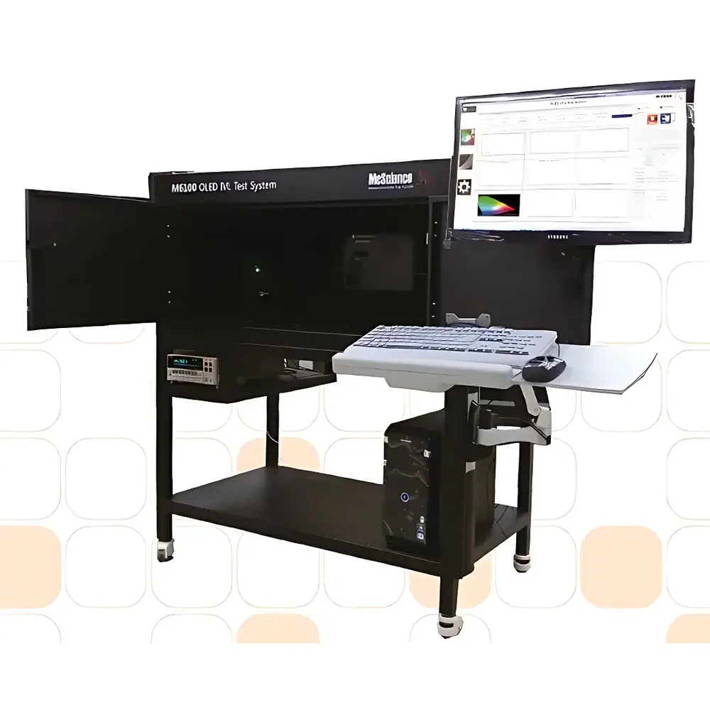
| Brand | McScience |
|---|---|
| Origin | South Korea |
| Model | M6100 |
| Instrument Type | Integrated Electroluminescence Characterization System for Organic and Emerging Light-Emitting Devices |
| Compliance | Designed for GLP-compliant lab environments |
| Electrical Source | Precision Source Measure Unit (SMU) |
| Optical Detection | Compatible with calibrated spectroradiometers and tristimulus colorimeters |
| Operating Environment | Light-tight enclosure with EMI-shielded chamber |
| Drive Modes | DC, pulsed, and programmable waveform injection |
| Sample Form Factor | Discrete devices, rigid/flexible substrates, micro-LED arrays, and active-matrix OLED panels |
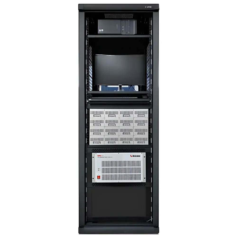
| Brand | McScience |
|---|---|
| Origin | South Korea |
| Model | OPD-LT |
| Channel Configuration | Multi-channel (configurable) |
| Spectral Range Options | UV to IR (200–1700 nm, selectable modules) |
| Compliance | ISO/IEC 17025-compatible test environment support |
| Software Control | PC-based with timestamped event logging and real-time degradation trend analysis |
| Operating Mode | Constant-bias or pulsed-bias stress testing under controlled ambient (N₂ glovebox or environmental chamber integration optional) |
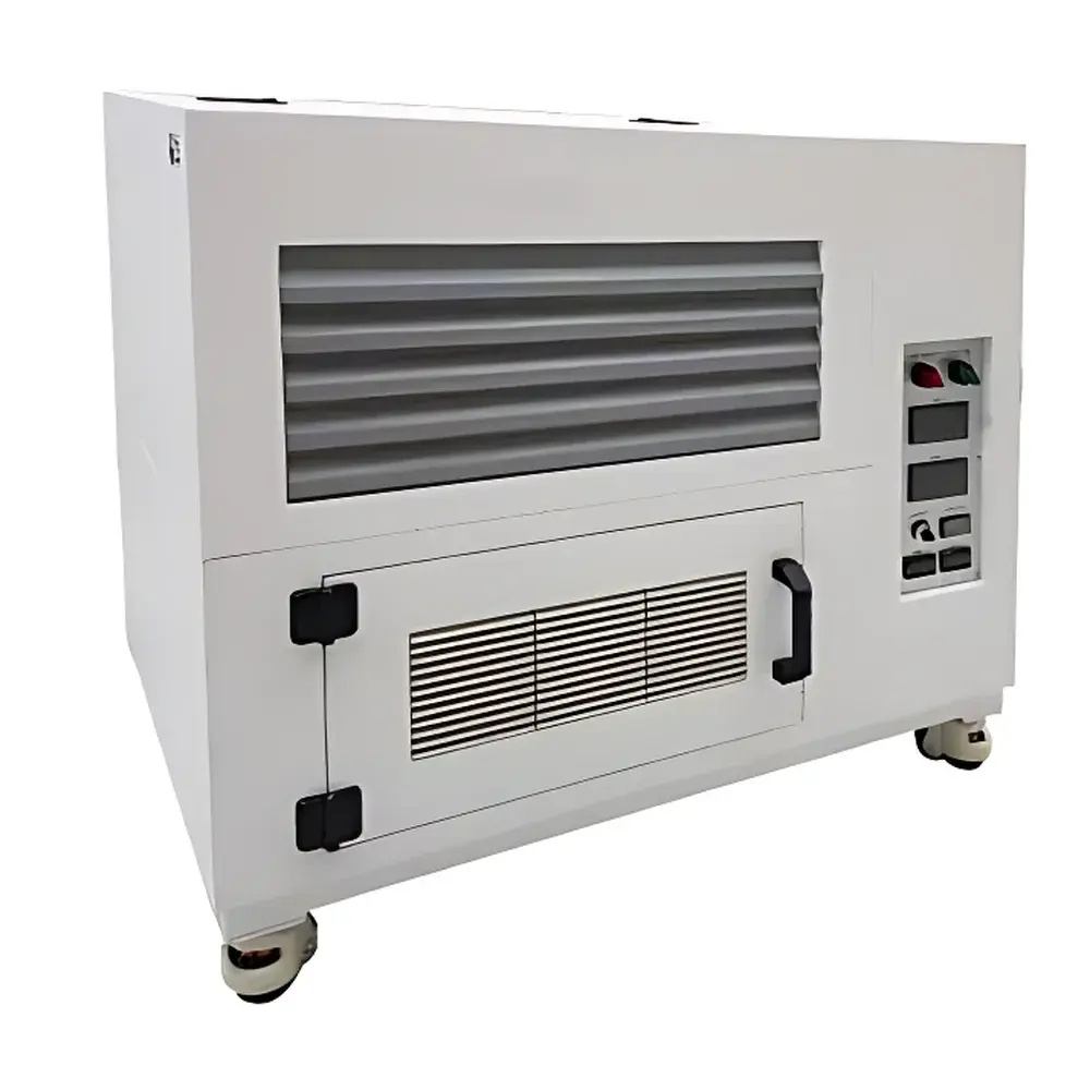
| Brand | McScience |
|---|---|
| Origin | South Korea |
| Model | K3600 |
| Light Source Options | Metal Halide, Plasma-based AAA, LED-based AAA Simulators |
| Environmental Control | Ambient-Temperature or Temperature/Humidity-Controlled Chamber Configurations |
| Test Capabilities | Continuous Illumination, High-Speed I-V Characterization, Multi-Channel Parallel Testing, Maximum Power Point Tracking (MPPT), Light-Induced Degradation (LID) Monitoring, Light Soaking Protocols |
| Compliance Support | ASTM E927, IEC 60904-9, IEC 61215 (for stability protocols), ISO 17025-aligned test reporting frameworks |
| Software | McScience Lifetest Suite with GLP/GMP-compliant audit trail, data versioning, and 21 CFR Part 11-ready user access controls |
| Brand | Oxford Instruments |
|---|---|
| Origin | United Kingdom |
| Manufacturer Type | Authorized Distributor |
| Origin Category | Imported |
| Model | Etch |
| Pricing | Upon Request |
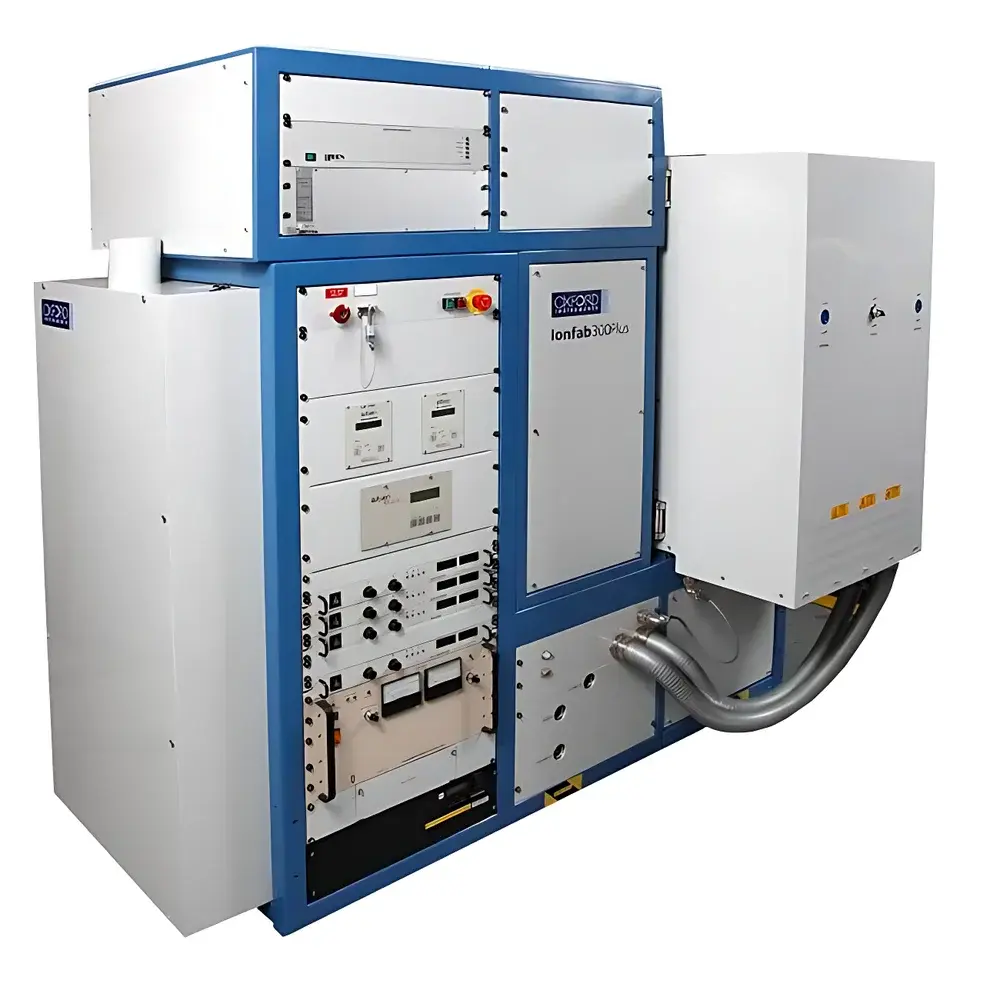
| Brand | Oxford Instruments |
|---|---|
| Origin | United Kingdom |
| Model | Ionfab 300 |
| Configuration Options | Direct-Load, Single-Wafer Transfer, Cassette-to-Cassette Transfer |
| Process Modes | Ion Beam Deposition (IBD), Ion Beam Etching (IBE), Co-deposition & Reactive IBE |
| Wafer Handling | 300 mm single-wafer or cluster-integrated |
| Surface Roughness | Sub-nanometer RMS (typical for IBD films) |
| Uniformity | ≤±1.5% across 300 mm wafer (process-dependent) |
| Reproducibility | CV < 2% for etch/deposition rate (run-to-run) |
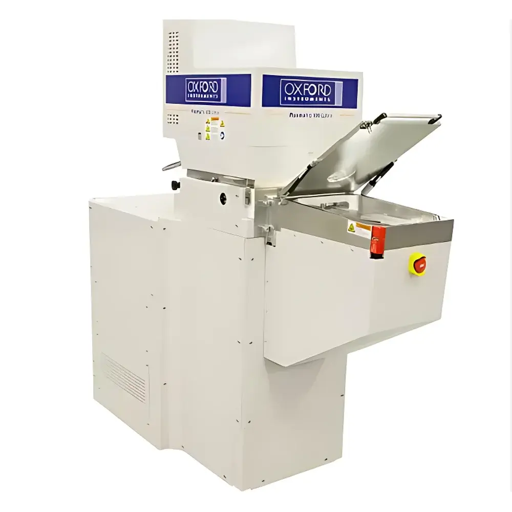
| Brand | Oxford Instruments |
|---|---|
| Origin | United Kingdom |
| Manufacturer Type | Authorized Distributor |
| Origin Category | Imported |
| Model | PlasmaPro 100 ALE |
| Pricing | Available Upon Request |
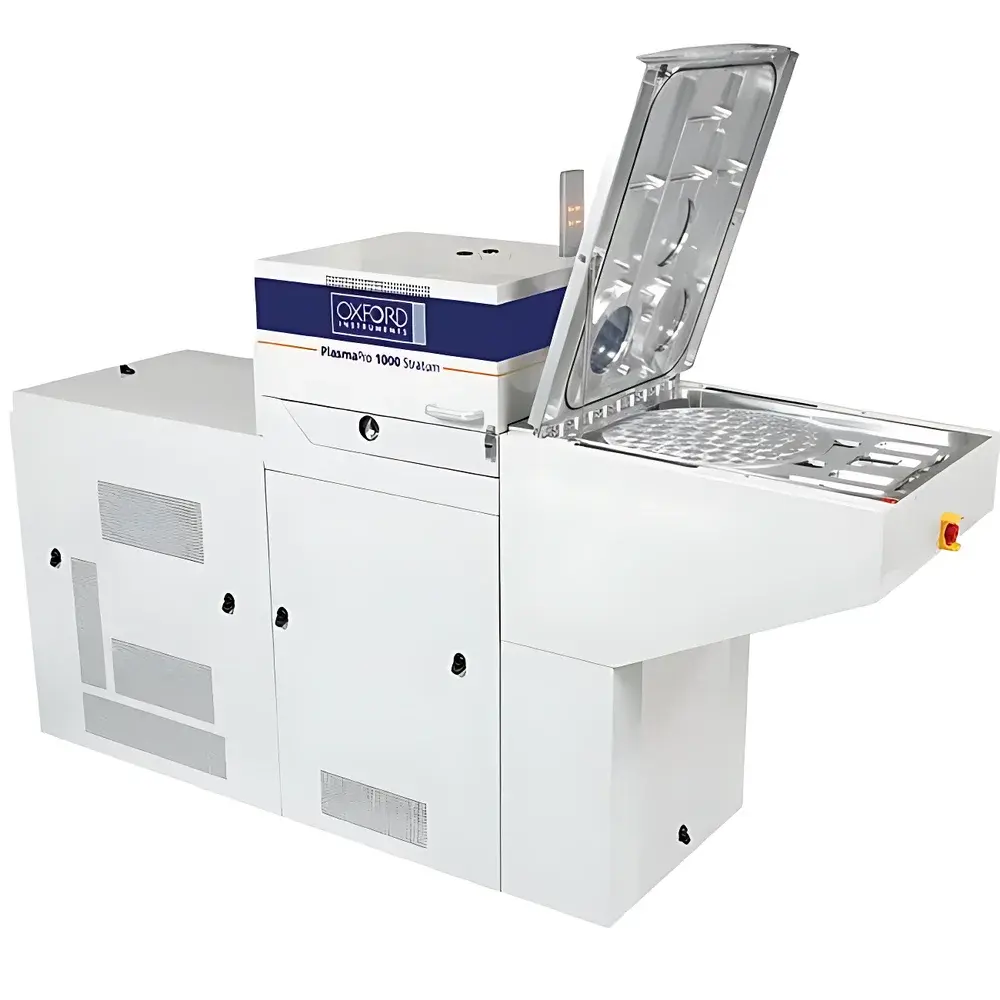
| Brand | Oxford Instruments |
|---|---|
| Origin | United Kingdom |
| Model | PlasmaPro 100 Estrelas |
| Substrate Size | 50–200 mm |
| Application Scope | Deep Silicon Etching (DSiE), MEMS, Advanced Packaging, Nanotechnology |
| Chamber Configuration | Single-chamber dual-mode (Bosch™ and cryogenic etching) |
| Process Flexibility | In-situ switchable between smooth sidewall, high-aspect-ratio, tapered via, and high-rate cavity etching |
| Key Hardware | Electrostatic/Heated chuck, optimized chamber liner, high-efficiency turbomolecular pump, fast-response mass flow controllers (MFCs), close-coupled RF delivery |
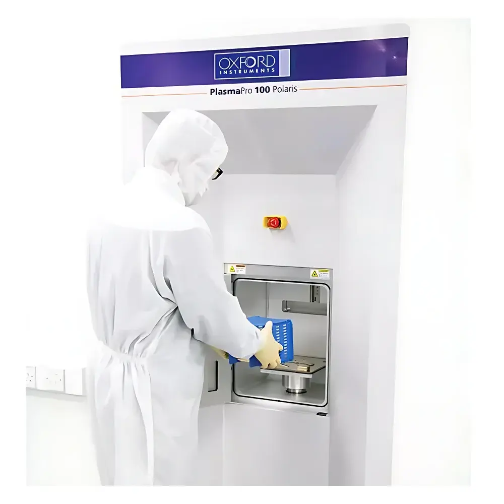
| Brand | Oxford Instruments |
|---|---|
| Origin | United Kingdom |
| Model | PlasmaPro 100 Polaris |
| Wafer Size | 100 mm (4-inch) |
| Plasma Source | Inductively Coupled Plasma (ICP) with Magnetic Confinement |
| Electrode Configuration | Actively Cooled Bottom Electrode |
| Chuck Type | Electrostatic Chuck (ESC) with DC Bias Control |
| Chamber Liner | Heated, Anodized Aluminum |
| Pumping System | High-Capacity Turbomolecular Pump with Cryo-Assisted Roughing |
| Process Gas Compatibility | Cl₂, BCl₃, SF₆, CHF₃, O₂, Ar, N₂, and custom gas mixtures |
| Control Architecture | PLC-based real-time process control with Ethernet-enabled SECS/GEM interface |
| Compliance | CE-marked |

| Brand | Oxford Instruments |
|---|---|
| Origin | United Kingdom |
| Model | NGP80 |
| Configuration Options | RIE, PECVD, RIE/PECVD |
| Wafer Handling | Up to 200 mm diameter wafers |
| Footprint | Compact (Small-Footprint) Design |
| Safety Compliance | SEMI S2/S8 |
| Control Architecture | Next-Generation Bus-Based Control System |
| User Interface | Enhanced Front-End Software with Integrated Diagnostics and Auto-Cleaning Protocol |
| Process Capabilities | Thin-film deposition (e.g., SiNₓ, SiO₂, a-Si:H), reactive ion etching, in-situ chamber conditioning |