
Semiconductor Instruments
Filter
Showing 541–570 of 852 results
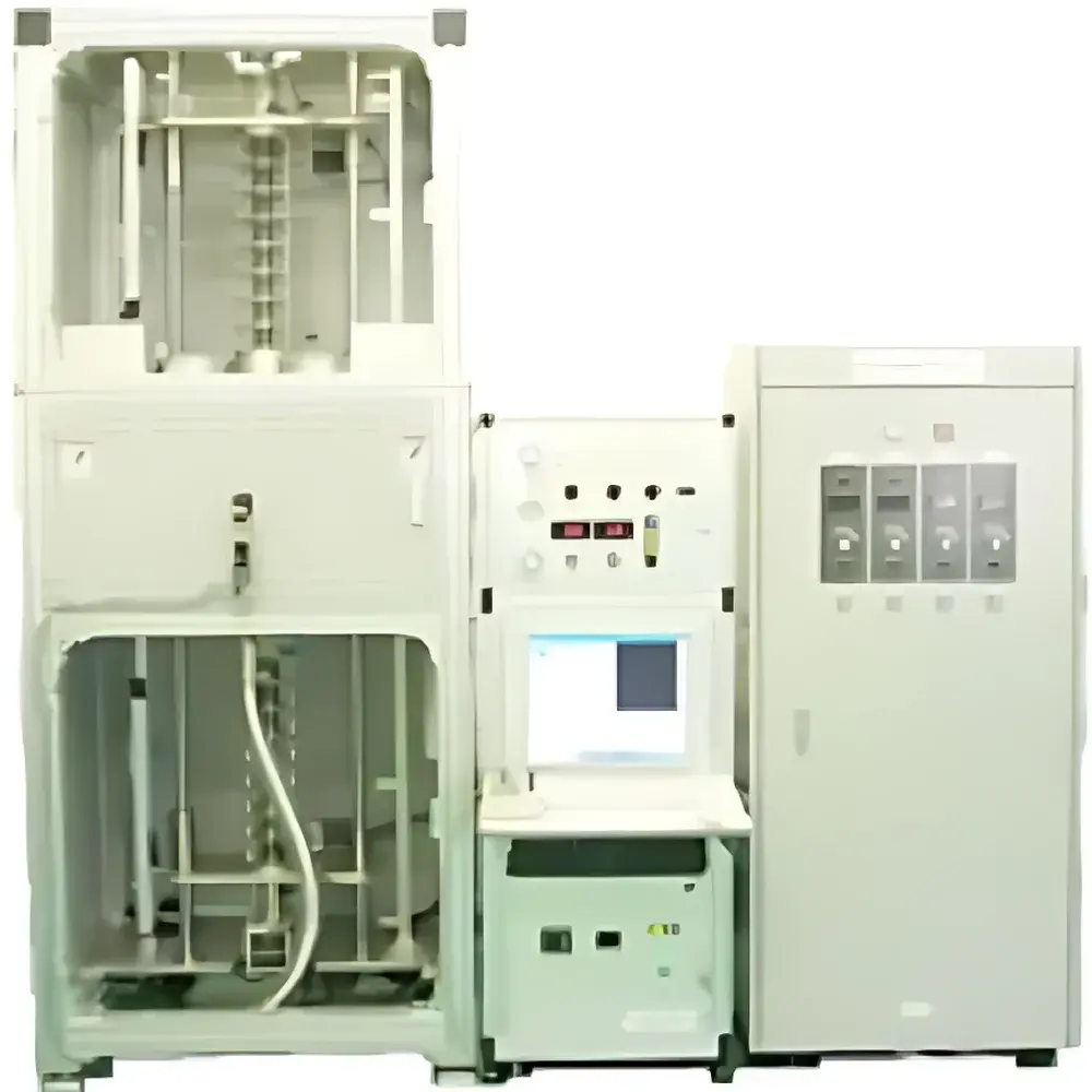
| Brand | CSC |
|---|---|
| Origin | Japan |
| Model | Magnetic Liquid Seal Type |
| Crystal Growth Capability | Single Crystal |
| Vacuum/Pressure Compatibility | Continuous Operation from High Vacuum to High Pressure |
| Heating System | Four-Mirror Optical Configuration |
| Control Interface | PC-Based Remote Control |
| Power Variants | FZ-T-4000-H (Standard), FZ-T-10000-H (High Power), FZ-T-12000-X (Super High Temperature) |
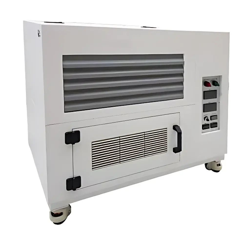
| Brand | McScience |
|---|---|
| Origin | South Korea |
| Model | K3600 |
| Light Source Options | Metal Halide, Plasma-based AAA, LED-based AAA Simulators |
| Environmental Control | Ambient-Temperature or Temperature/Humidity-Controlled Chamber Configurations |
| Test Capabilities | Continuous Illumination, High-Speed I-V Characterization, Multi-Channel Parallel Testing, Maximum Power Point Tracking (MPPT), Light-Induced Degradation (LID) Monitoring, Light Soaking Protocols |
| Compliance Support | ASTM E927, IEC 60904-9, IEC 61215 (for stability protocols), ISO 17025-aligned test reporting frameworks |
| Software | McScience Lifetest Suite with GLP/GMP-compliant audit trail, data versioning, and 21 CFR Part 11-ready user access controls |
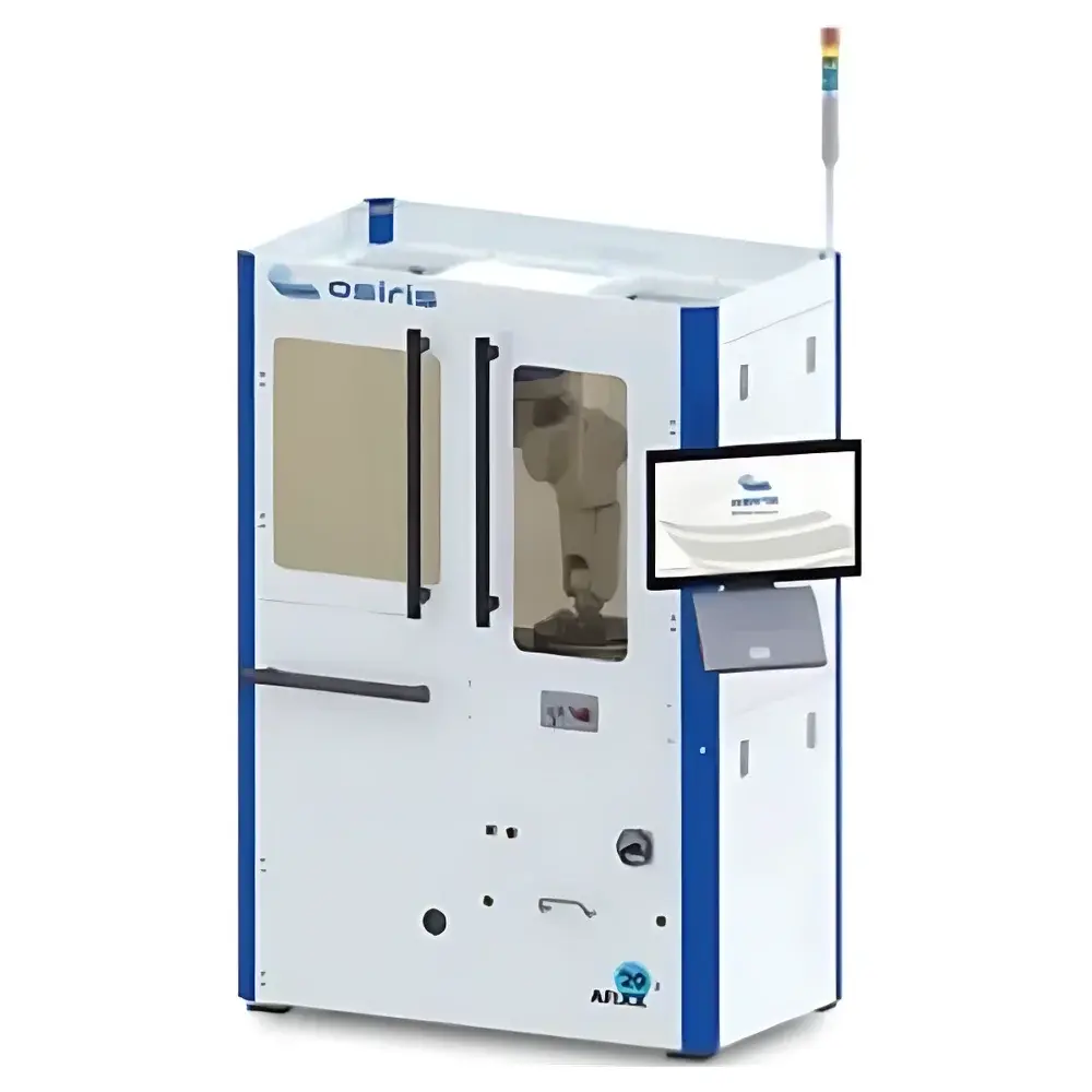
| Brand | Osiris |
|---|---|
| Origin | Germany |
| Model | AFIXX 30s |
| Maximum Wafer Size | 200 mm |
| Temperature Range | Up to 650 °C (Independent Top/Bottom Plate Control) |
| Bonding Processes Supported | Thermal Compression, Adhesive Bonding, Glass Frit Bonding, Anodic Bonding, Eutectic Bonding, Direct Si–Si Bonding, SOI Bonding |
| Compatibility | Silicon, Compound Semiconductors (GaAs, SiC, GaN), Glass, Quartz, and SOI Wafers |
| System Architecture | Modular Bonding Chamber with In-Situ Alignment & Activation |
| Nanopatterning Capability | Integrated Nanoimprint Functionality |
| Compliance | Designed for GLP/GMP-aligned R&D and low-volume production environments |
| Operating Interface | Windows 10-based GUI with 22" Touchscreen HMI |
| Safety | Transparent Viewport Door for Real-Time Process Monitoring |
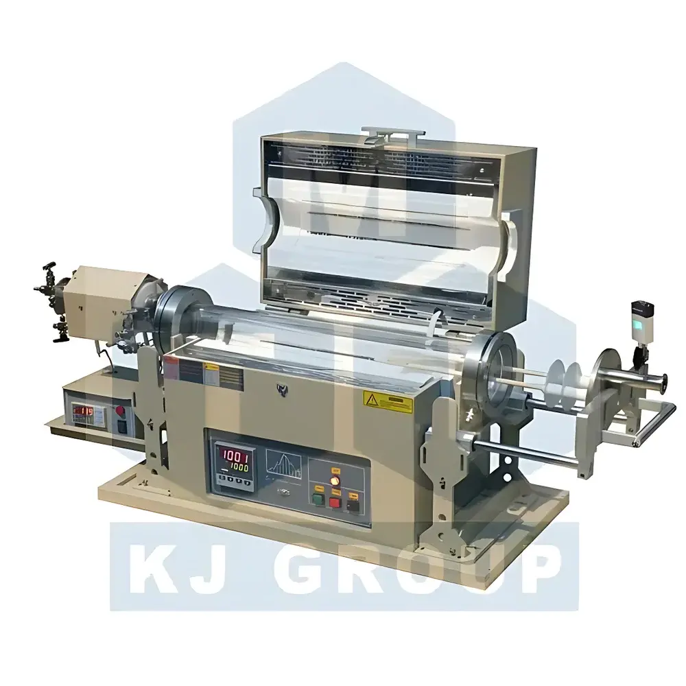
| Brand | Hefei Kejing |
|---|---|
| Origin | Anhui, China |
| Manufacturer Type | Authorized Distributor |
| Region of Manufacture | Domestic (China) |
| Model | OTF-1200X-4-NW |
| Quotation | Upon Request |
| Main Tube | 100 mm OD × 94 mm ID × 750 mm L (Fused Quartz) |
| Max Operating Temp (Main Zone) | 1100 °C (<2 hr), 1000 °C continuous |
| Preheat Zone | 30 mm OD × 150 mm L (Stainless Steel), RT–600 °C continuous |
| Heating Zones | Main: 440 mm (100 mm isothermal) |
| Preheat | 150 mm |
| Max Ramp Rate | 20 °C/min (both zones) |
| Power Supply | 220 V AC, 50/60 Hz, single-phase |
| Max Power | 3.6 kW |
| Cooling | Water-cooled KF25 flange with integrated seal cooling |
| Gas Inlets | Four 1/8" Swagelok ports on left flange |
| Vacuum Compatibility | KF25 interface for turbomolecular or rotary vane pump |
| Control System | Dual independent PID controllers, 30-segment programmable ramp-soak profiles, K-type thermocouples, ±1 °C accuracy |
| Optional | PC-based temperature control software (USB/RS485) |
| Dimensions (closed) | 1580 × 458 × 585 mm (62" × 18" × 23") |
| (fully extended) | 2040 × 458 × 585 mm (80" × 18" × 23") |
| Weight | 110 kg |
| Warranty | 12 months parts & labor (excludes consumables: quartz tube, O-rings, heating elements) |
| Safety Certification | UL-listed electrical components (>24 V) |
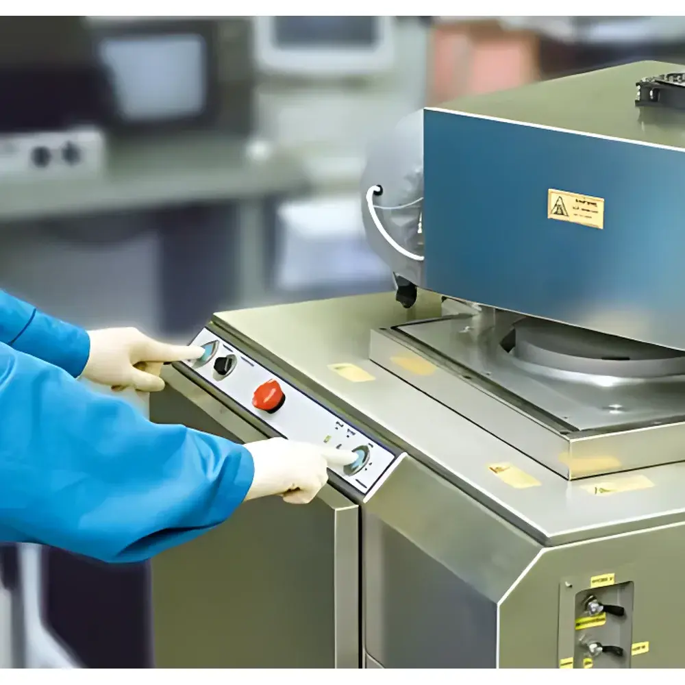
| Brand | Oxford Instruments |
|---|---|
| Origin | United Kingdom |
| Model | ALD OpAL |
| Substrate Size | Up to 200 mm |
| Process Temperature | Up to 200 °C |
| Precursor Sources | Up to 4 (liquid or solid) |
| Plasma-Enhanced ALD Capability | Optional, field-upgradable |
| Chamber Design | Direct-load, open-frame thermal ALD platform |
| Safety Integration | Compatible with N₂-purged gloveboxes and exhaust hoods |
| Service Support | Lifetime process support, including new recipe development and material-specific optimization guidance |
| Brand | Oxford Instruments |
|---|---|
| Origin | United Kingdom |
| Manufacturer Type | Authorized Distributor |
| Origin Category | Imported |
| Model | Etch |
| Pricing | Upon Request |
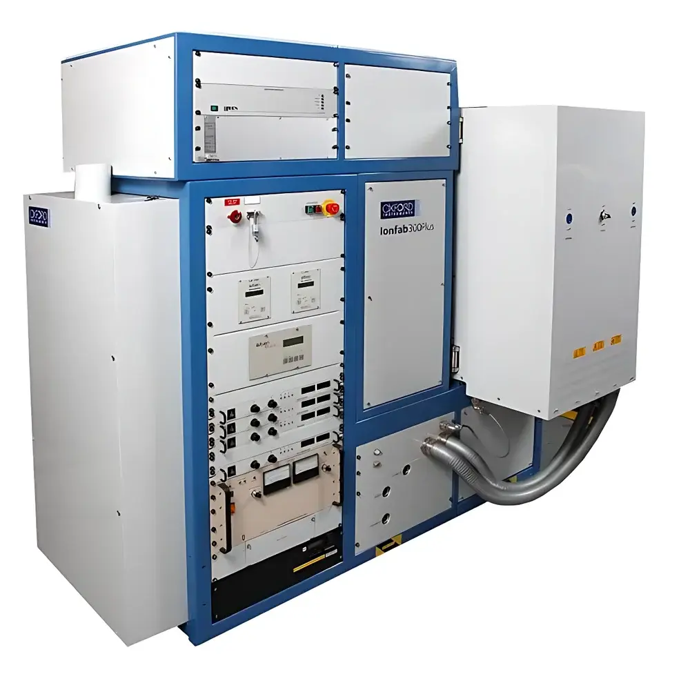
| Brand | Oxford Instruments |
|---|---|
| Origin | United Kingdom |
| Model | Ionfab 300 |
| Configuration Options | Direct-Load, Single-Wafer Transfer, Cassette-to-Cassette Transfer |
| Process Modes | Ion Beam Deposition (IBD), Ion Beam Etching (IBE), Co-deposition & Reactive IBE |
| Wafer Handling | 300 mm single-wafer or cluster-integrated |
| Surface Roughness | Sub-nanometer RMS (typical for IBD films) |
| Uniformity | ≤±1.5% across 300 mm wafer (process-dependent) |
| Reproducibility | CV < 2% for etch/deposition rate (run-to-run) |
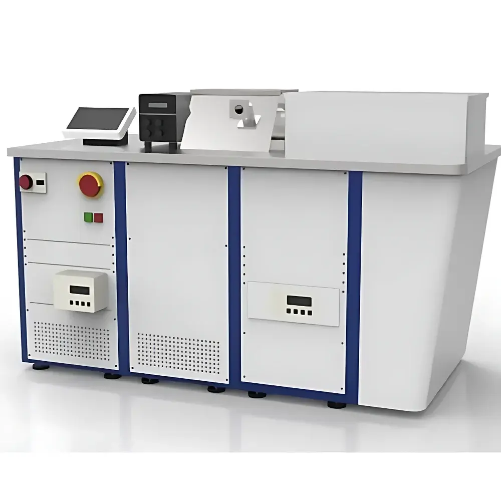
| Brand | Oxford Instruments |
|---|---|
| Model | Plasmalab 133 |
| Maximum Wafer Size | 300 mm (330 mm chuck) |
| RF Power | 600 W, 13.56 MHz |
| Electrode Temperature Control | 10 °C – 80 °C (water-cooled) |
| Endpoint Detection | Verity Optical Emission Spectroscopy (OES), 200–800 nm |
| Gas Delivery | 8-line manifold with 7 Mass Flow Controllers (MFCs): Ar (100 sccm), Cl₂ (100 sccm), BCl₃ (100 sccm), N₂O (200 sccm), CHF₃ (200 sccm), NH₃ (100 sccm), CH₄ (50 sccm) |
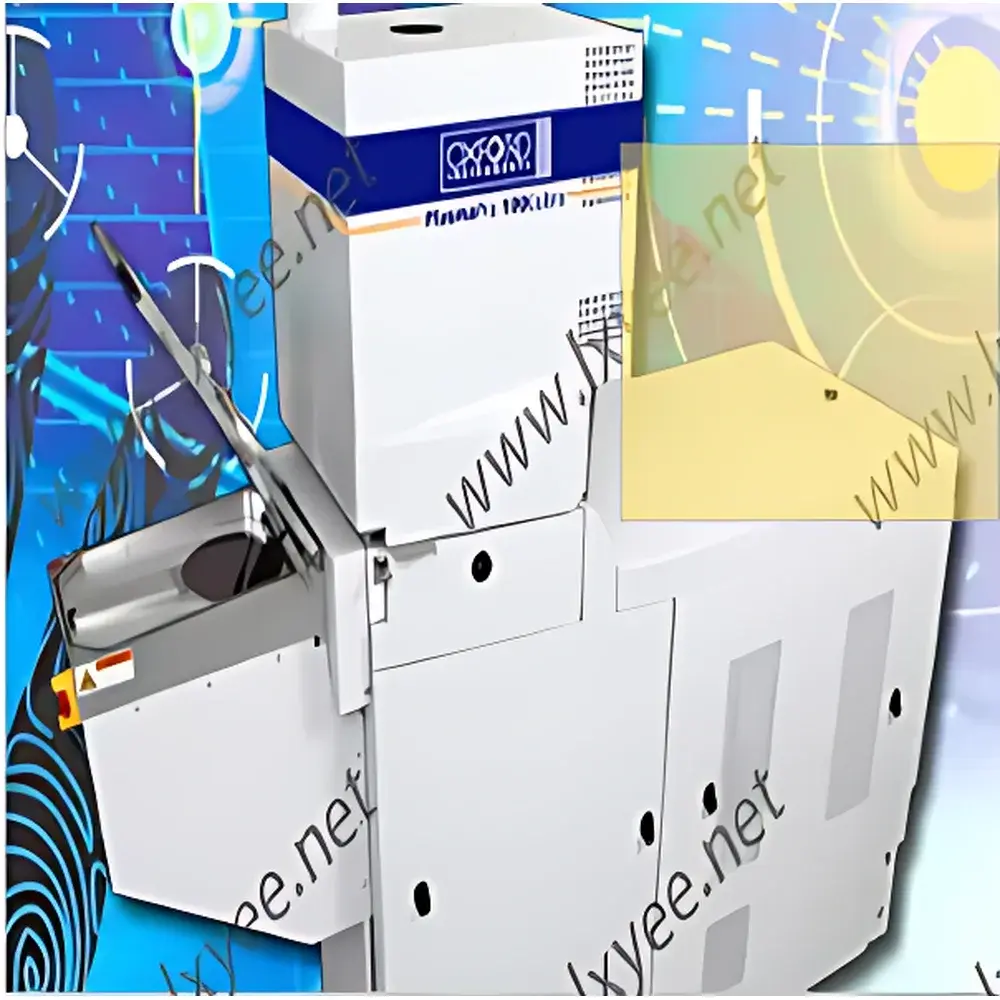
| Brand | Oxford Instruments |
|---|---|
| Origin | United Kingdom |
| Model | Plasmalab System 100 |
| Wafer Handling | Up to 200 mm (8") single-wafer or batch (6 × 50 mm), cassette-to-cassette transfer via load-lock chamber |
| Substrate Temperature Range | –150 °C to +700 °C |
| Gas Delivery | Optional 6- or 12-channel gas manifold (remotely mounted) |
| In-situ Endpoint Detection | Laser interferometry and/or optical emission spectroscopy (OES) compatible |
| Integration Capability | Cluster tool ready with robotic wafer handling |
| Process Flexibility | Reactive ion etching (RIE), inductively coupled plasma (ICP), electron cyclotron resonance (ECR), and plasma-enhanced chemical vapor deposition (PECVD) modes |
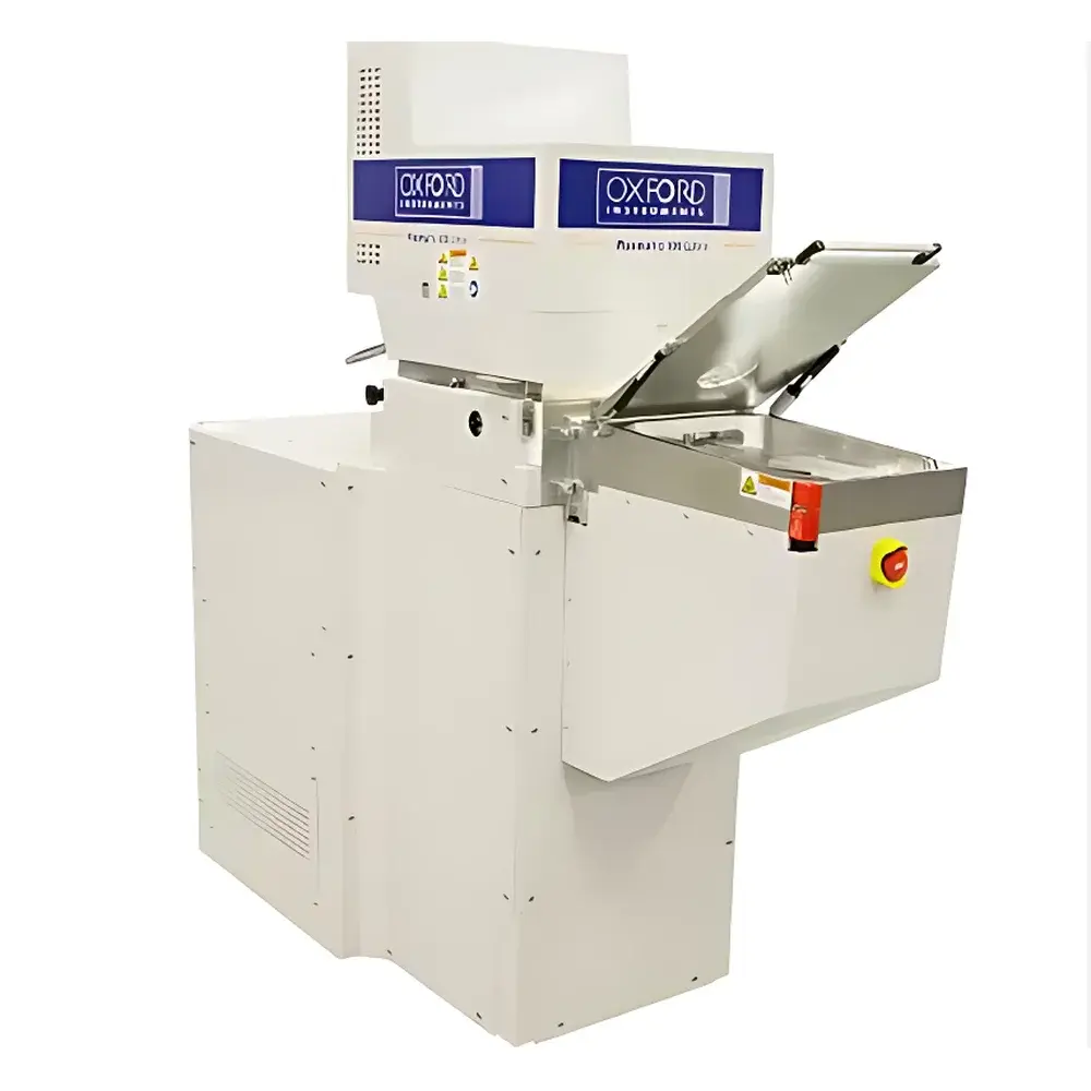
| Brand | Oxford Instruments |
|---|---|
| Origin | United Kingdom |
| Manufacturer Type | Authorized Distributor |
| Origin Category | Imported |
| Model | PlasmaPro 100 ALE |
| Pricing | Available Upon Request |
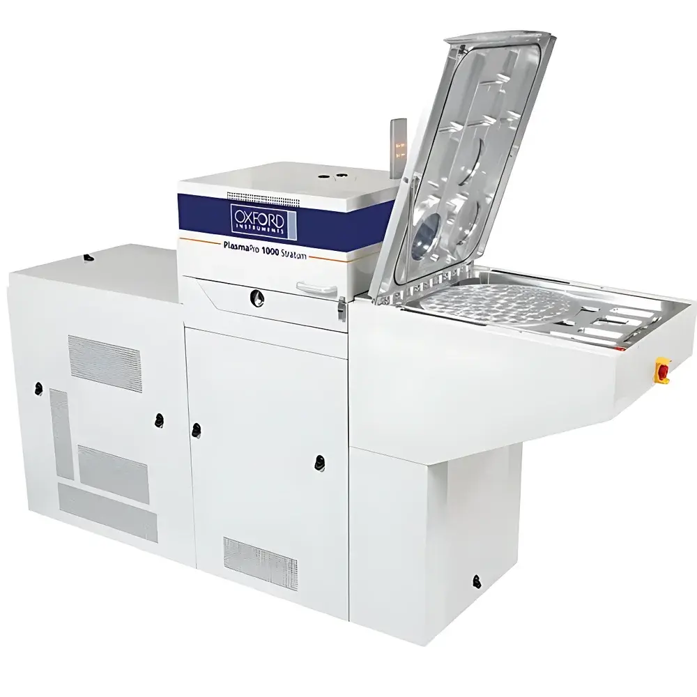
| Brand | Oxford Instruments |
|---|---|
| Origin | United Kingdom |
| Model | PlasmaPro 100 Estrelas |
| Substrate Size | 50–200 mm |
| Application Scope | Deep Silicon Etching (DSiE), MEMS, Advanced Packaging, Nanotechnology |
| Chamber Configuration | Single-chamber dual-mode (Bosch™ and cryogenic etching) |
| Process Flexibility | In-situ switchable between smooth sidewall, high-aspect-ratio, tapered via, and high-rate cavity etching |
| Key Hardware | Electrostatic/Heated chuck, optimized chamber liner, high-efficiency turbomolecular pump, fast-response mass flow controllers (MFCs), close-coupled RF delivery |
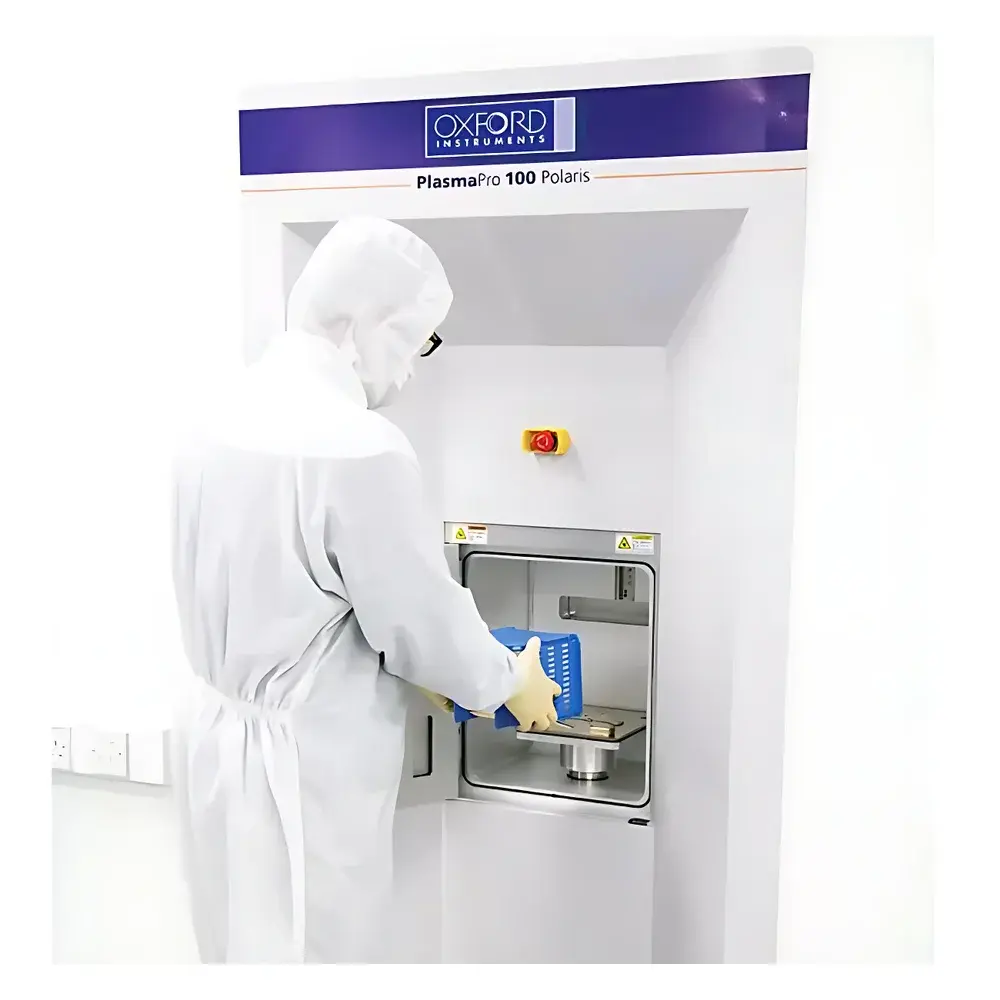
| Brand | Oxford Instruments |
|---|---|
| Origin | United Kingdom |
| Model | PlasmaPro 100 Polaris |
| Wafer Size | 100 mm (4-inch) |
| Plasma Source | Inductively Coupled Plasma (ICP) with Magnetic Confinement |
| Electrode Configuration | Actively Cooled Bottom Electrode |
| Chuck Type | Electrostatic Chuck (ESC) with DC Bias Control |
| Chamber Liner | Heated, Anodized Aluminum |
| Pumping System | High-Capacity Turbomolecular Pump with Cryo-Assisted Roughing |
| Process Gas Compatibility | Cl₂, BCl₃, SF₆, CHF₃, O₂, Ar, N₂, and custom gas mixtures |
| Control Architecture | PLC-based real-time process control with Ethernet-enabled SECS/GEM interface |
| Compliance | CE-marked |
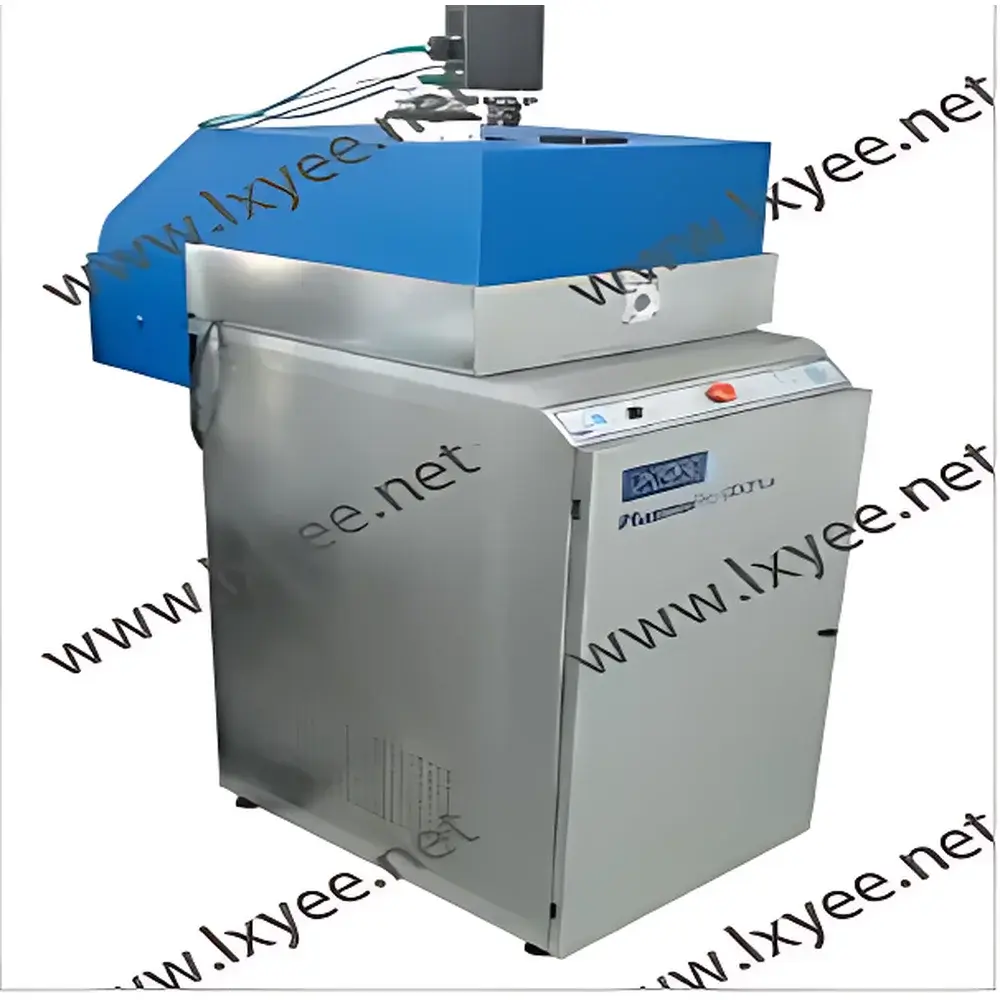
| Brand | Oxford Instruments |
|---|---|
| Origin | United Kingdom |
| Model | PlasmaPro 800 RIE |
| Category | Dry Process Equipment for Semiconductor Fabrication |
| Etching Principle | Reactive Ion Etching (RIE) with optional Plasma Enhanced (PE) mode |
| Substrate Compatibility | Up to 300 mm wafers and batch processing |
| Electrode Configuration | Large-area lower electrode with liquid cooling and/or resistive heating |
| Endpoint Detection | Laser interferometry and/or optical emission spectroscopy (OES) |
| Gas Delivery | Configurable gas cabinet with 4-, 8-, or 12-channel options |
| Vacuum System | Proximal turbomolecular pumping |
| Temperature Control | Precision substrate temperature regulation (±0.5 °C typical stability) |
| Compliance | Designed for GLP/GMP-aligned process documentation |

| Brand | Oxford Instruments |
|---|---|
| Origin | United Kingdom |
| Model | NGP80 |
| Configuration Options | RIE, PECVD, RIE/PECVD |
| Wafer Handling | Up to 200 mm diameter wafers |
| Footprint | Compact (Small-Footprint) Design |
| Safety Compliance | SEMI S2/S8 |
| Control Architecture | Next-Generation Bus-Based Control System |
| User Interface | Enhanced Front-End Software with Integrated Diagnostics and Auto-Cleaning Protocol |
| Process Capabilities | Thin-film deposition (e.g., SiNₓ, SiO₂, a-Si:H), reactive ion etching, in-situ chamber conditioning |
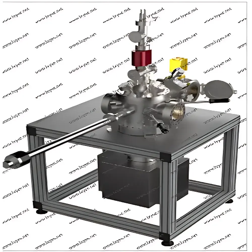
| Brand | PancanNano |
|---|---|
| Origin | Germany |
| Manufacturer Type | Authorized Distributor |
| Product Category | Imported Equipment |
| Model | SII |
| Product Type | High-Energy Single-Ion Implanter |
| Application Domain | IC & Quantum Device Fabrication |
| Implantation Energy | Custom-configurable per ion species (e.g., 1–100 keV) |
| Ion Dose Range | 1 to 10⁶ ions per site (single-ion counting mode) |
| Wafer Compatibility | Up to 150 mm (6″) substrates, compatible with diced chips and bulk crystals |
| Supported Ions | H⁺, N⁺, O⁺, Si⁺, P⁺, B⁺, As⁺, Te⁺, Ar⁺ (and other singly charged species via optional source modules) |
| Dimensions (L × W × H) | 2.4 m × 1.8 m × 2.2 m (fully shielded vacuum enclosure) |
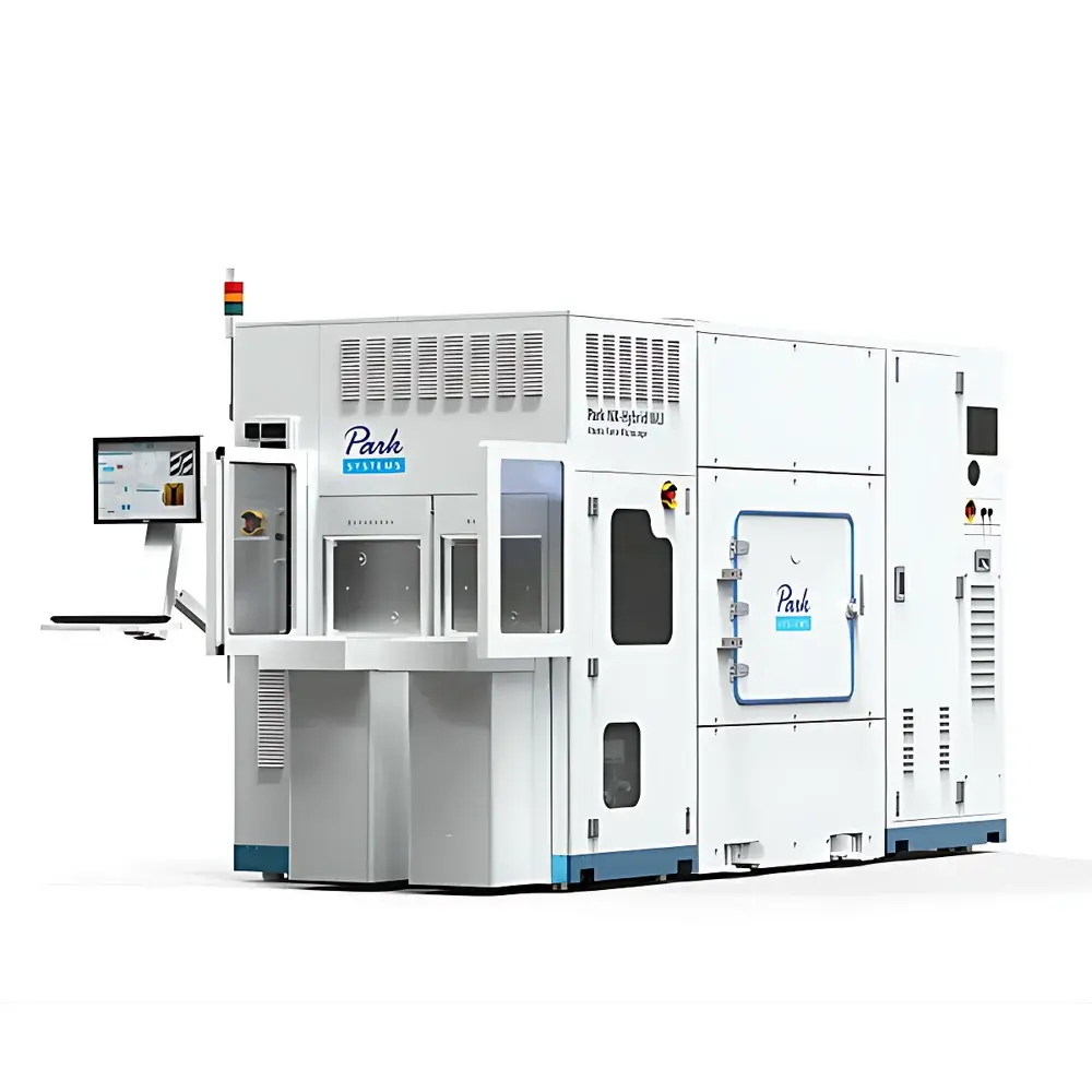
| Brand | Park SYSTEMS |
|---|---|
| Origin | South Korea |
| Model | NX-Hybrid WLI |
| Wafer Compatibility | 300 mm (fully backward-compatible with 200 mm and smaller wafers) |
| Instrument Category | Optical Defect Inspection & Hybrid Metrology System |
| Primary Application | In-line semiconductor process monitoring and defect characterization |
| Core Technology Integration | Co-registered AFM + WLI on single platform |
| Measurement Capability | Sub-ångström vertical resolution (AFM), nanometer-level lateral resolution, µm-to-mm field-of-view (WLI) |
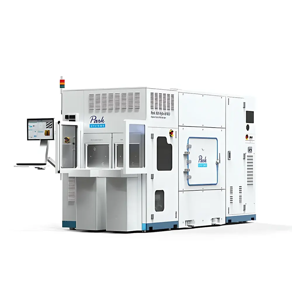
| Brand | Park SYSTEMS |
|---|---|
| Origin | South Korea |
| Model | NX-Hybrid WLI |
| Primary Technology | Integrated White Light Interferometry (WLI) and Atomic Force Microscopy (AFM) |
| Optical Modes | WLI & Phase-Shifting Interferometry (PSI) |
| Objective Lenses | 2.5×, 10×, 20×, 50×, 100× (motorized turret) |
| Interferometric Objective Type | Mirau |
| Measurement Principle | Coherence scanning interferometry with sub-nanometer vertical resolution |
| Application Domain | Semiconductor front-end & back-end process control, advanced packaging metrology, wafer-level defect review, CMP characterization, GLP/GMP-compliant R&D and inline QA |
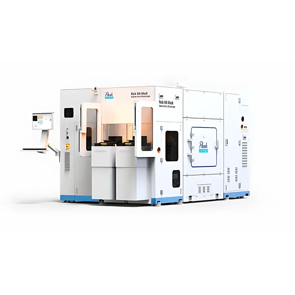
| Brand | Park SYSTEMS |
|---|---|
| Origin | South Korea |
| Model | NX-Mask |
| Application | EUV photomask defect repair and metrology |
| Technology | Non-contact atomic force microscopy (AFM) |
| Key Capabilities | Defect detection, nanoscale mechanical removal, post-repair 3D topography verification |
| Compliance | Designed for cleanroom-integrated semiconductor mask shops |
| Deployment | Dual-pod compatible for inline EUV reticle handling |
| Operational Environment | Ambient air, no vacuum, no beam-induced charging, no chemical reagents |
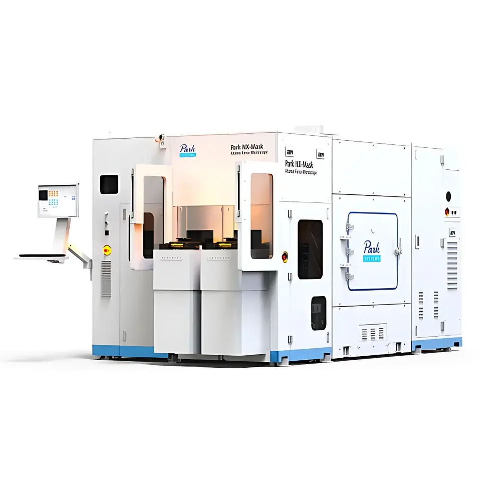
| Brand | Park SYSTEMS |
|---|---|
| Origin | South Korea |
| Model | NX-Mask |
| Application | EUV photomask defect repair, AFM-based nanomechanical removal and verification |
| Compliance | Designed for ISO 14644-1 Class 1–5 cleanroom integration |
| Software | XEI™ with automated defect-to-repair workflow, audit-trail logging per FDA 21 CFR Part 11 requirements |
| Repair Mechanism | Non-contact, voltage-controlled AFM tip nanoscrubbing and localized mechanical lift-off |
| Resolution | Sub-5 nm lateral resolution in topography and phase imaging |
| Sample Handling | Dual-pod EUV reticle cassette compatibility (SEMI F47 compliant) |
| Vacuum Requirement | None |
| Charging Risk | Electrostatically neutral operation |
| Chemical Usage | Dry, solvent-free process |
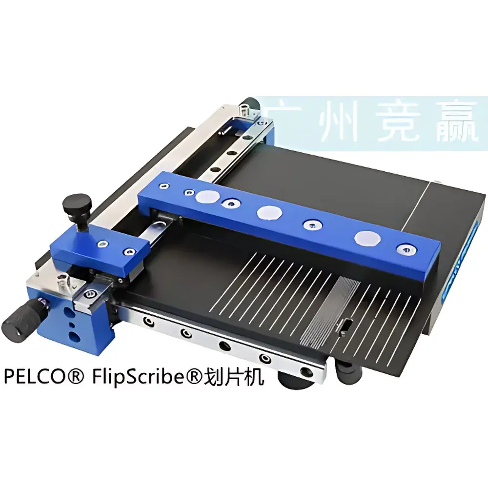
| Brand | Ted Pella |
|---|---|
| Origin | USA |
| Manufacturer Type | Authorized Distributor |
| Origin Category | Imported |
| Model | FlipScribe |
| Maximum Scribing Speed | Manual Operation |
| Application Scope | Semiconductor Wafer Dicing, Backside Alignment Scribing, Brittle Substrate Preparation |
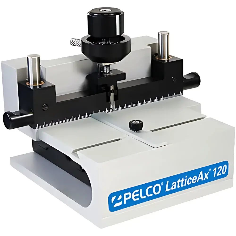
| Brand | Ted Pella |
|---|---|
| Origin | USA |
| Manufacturer Type | Authorized Distributor |
| Origin Category | Imported |
| Model | LatticeAx 120 |
| Maximum Linear Scribing Speed | 100 mm/min |
| Application Scope | Semiconductor Wafers, Compound Semiconductors, Optical Substrates |
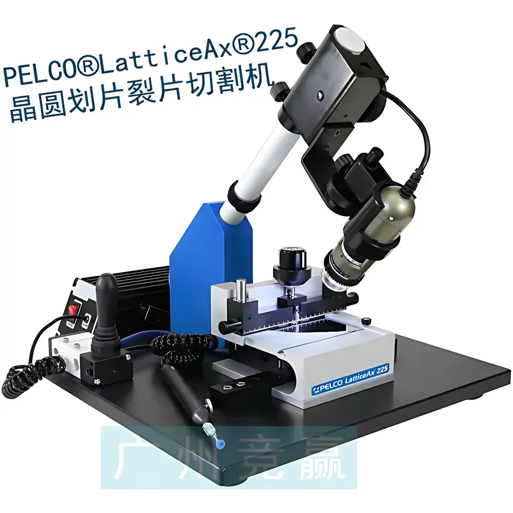
| Brand | Ted Pella |
|---|---|
| Origin | USA |
| Manufacturer Type | Authorized Distributor |
| Product Origin | Imported |
| Model | LatticeAx 225 |
| Maximum Scribe Line Speed | 600 mm/min |
| Application Scope | Semiconductor Wafers, MEMS, Optoelectronics, and Thin-Film Devices |
| Positioning Accuracy | ±20 µm |
| Scribe Impression Length | <1 mm |
| Impression Width | ~10 µm |
| Imaging System | USB 2.0 Digital Microscope with Polarizing Filter and Real-Time Capture Software |
| Vacuum Fixation | Pneumatically Actuated Valve-Controlled Pump |
| Sample Compatibility | Si, SiC, GaAs, Sapphire, Glass, Quartz, and Thin-Film Substrates (Ø50–300 mm, Thickness 100–1000 µm) |
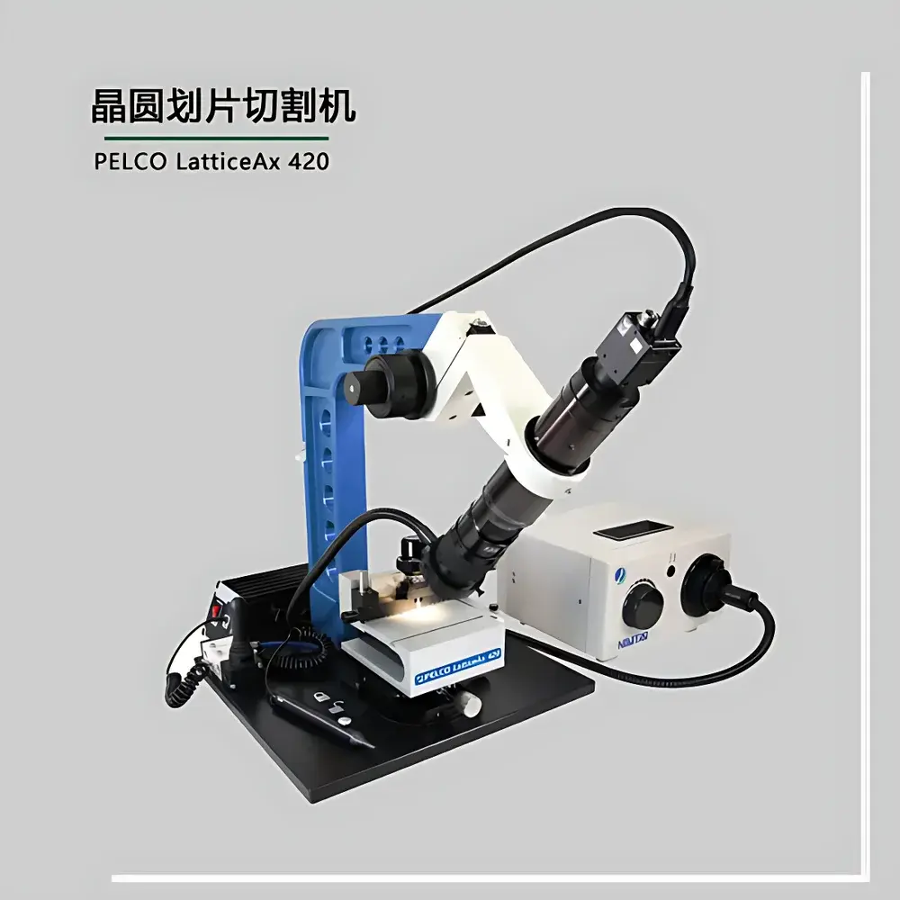
| Origin | USA |
|---|---|
| Manufacturer Type | Distributor |
| Origin Category | Imported |
| Model | PELCO LatticeAx 420 |
| Price Range | USD 0–15,000 |
| Maximum Scribe Speed | 500–600 mm/min |
| Application Scope | Laboratory Use |
| Positioning Accuracy | ±10 µm |
| Indentation Step Resolution | 5 µm |
| Optical Magnification | 0.58–7× (zoom, parfocal, monocular) |
| Camera | Color CCD |
| Diamond Scribing Tip | Polished Single-Point Diamond |
| Focusing Mechanism | Coarse + Fine Focus Stage |
| Footprint | Compact Industrial Platform |
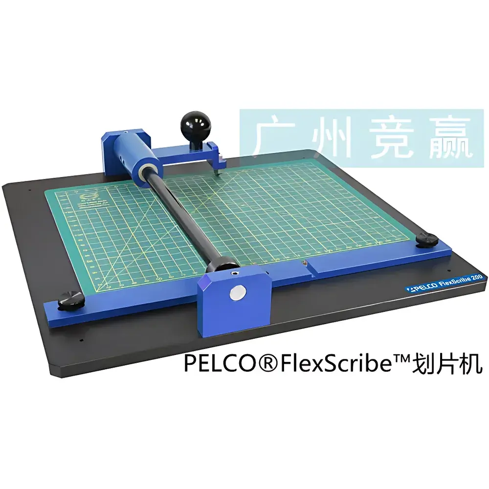
| Brand | Ted Pella |
|---|---|
| Origin | USA |
| Model | FlexScribe |
| Sample Size Range | 5 mm to 300 mm |
| Blade Options | Tungsten Carbide (#54346), Diamond (#54343), Deep-Cut Wheel (#54344) |
| Primary Application | Semiconductor Wafer and Brittle Material Scribing |
| Operation Mode | Manual Linear Scribing Only |
| Compliance | Designed for ISO/IEC 17025-aligned lab environments, compatible with GLP documentation workflows |
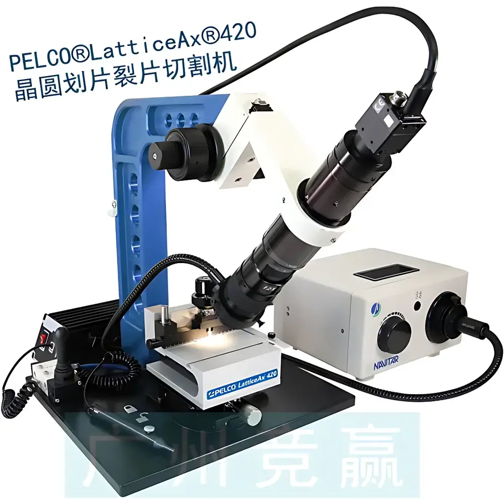
| Brand | Ted Pella |
|---|---|
| Origin | USA |
| Manufacturer Type | Authorized Distributor |
| Origin Category | Imported |
| Model | LatticeAx 420 |
| Maximum Linear Scribing Speed | 600 µm/s |
| Application Scope | Semiconductor Wafers, MEMS, Compound Semiconductors (SiC, GaN), Optical Substrates, and Research-Scale Device Fabrication |
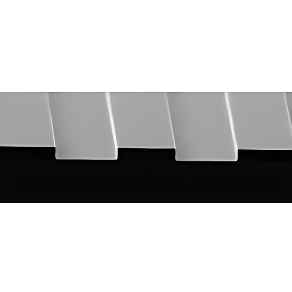
| Brand | MicroChem Corp |
|---|---|
| Origin | USA |
| Product Type | Photoimageable epoxy-based wafer bonding adhesive |
| Series | PermiNex™ 1000 and 2000 |
| Temperature Resistance | <200 °C cure |
| Resolution | High-resolution patterning |
| Aspect Ratio | Up to 3:1 |
| Developer Compatibility | Aqueous alkaline solutions |
| Substrate Adhesion | Silicon, glass, quartz, SiO₂, SiNₓ |
| Shelf Life Storage | 4–21 °C |
| Corrosivity | Low metal ion contamination |
| Conformality | Void-free, conformal interface |
| Edge Acuity | Sharp, crack-free pattern edges |
| Reliability | Qualified for HAST (JESD22-A110) and TCT (JESD22-A104) |
| Seal Integrity | High hermeticity post-bond |
| Process Compatibility | Compatible with dicing, laser welding, and backend packaging steps |
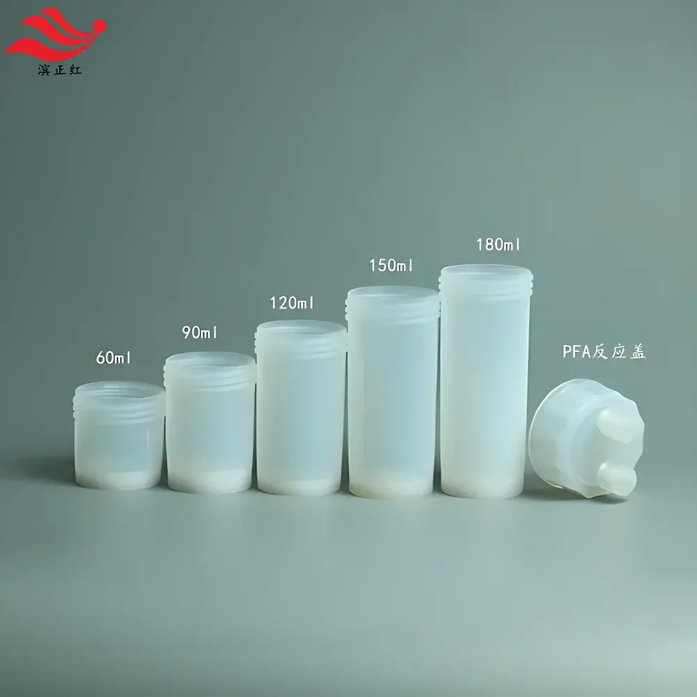
| Brand | Binzhenghong |
|---|---|
| Origin | Jiangsu, China |
| Manufacturer Type | Direct Producer |
| Country of Origin | China |
| Capacity Options | 60 mL, 90 mL, 120 mL, 150 mL, 180 mL |
| Pricing | Upon Request |
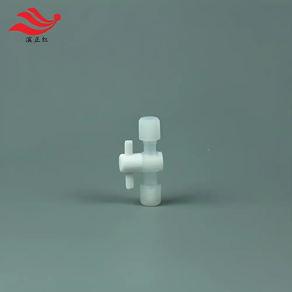
| Brand | Binzhenghong |
|---|---|
| Model | 1/4″ PFA Three-Way Valve |
| Origin | Jiangsu, China |
| Manufacturer Type | Direct Manufacturer |
| Country of Origin | China |
| Pricing | Upon Request |
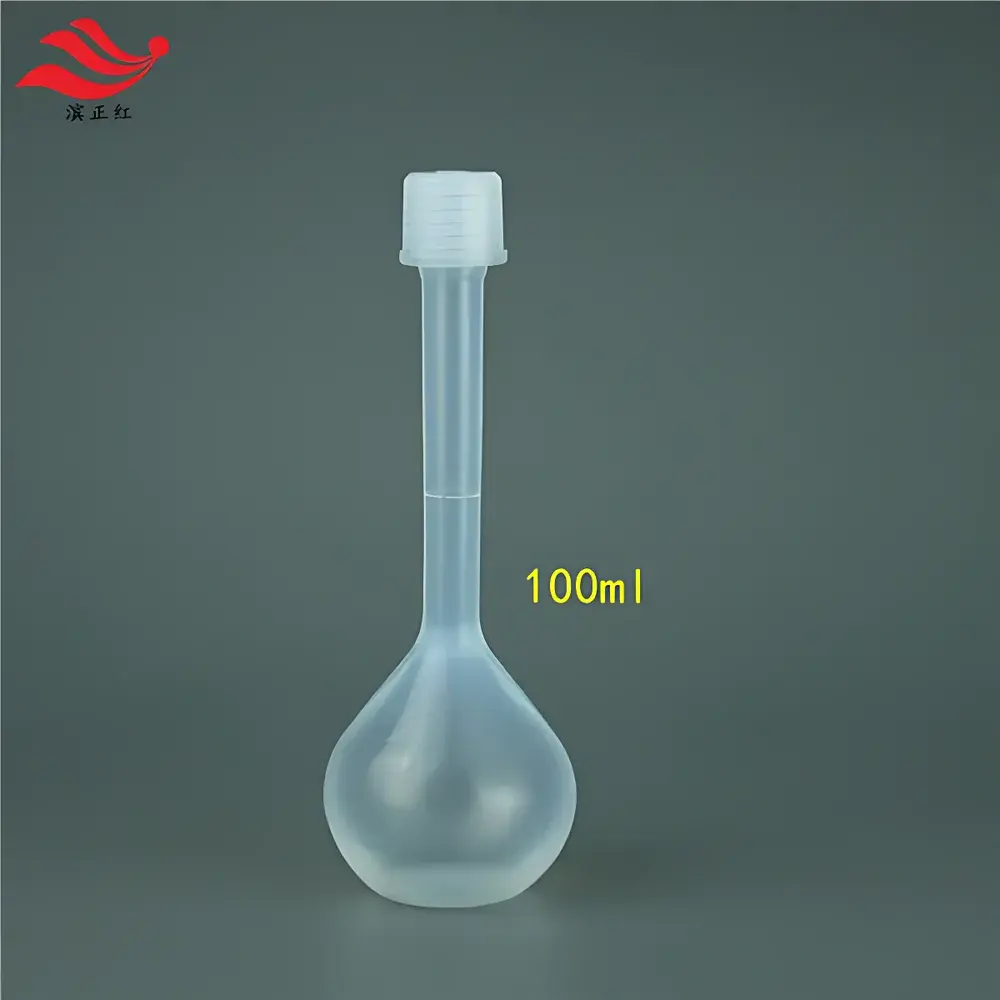
| Brand | Binzhenghong |
|---|---|
| Origin | Jiangsu, China |
| Manufacturer Type | Direct Producer |
| Classification | Domestic |
| Capacity Range | 10 mL to 1000 mL |
| Pricing | Upon Request |
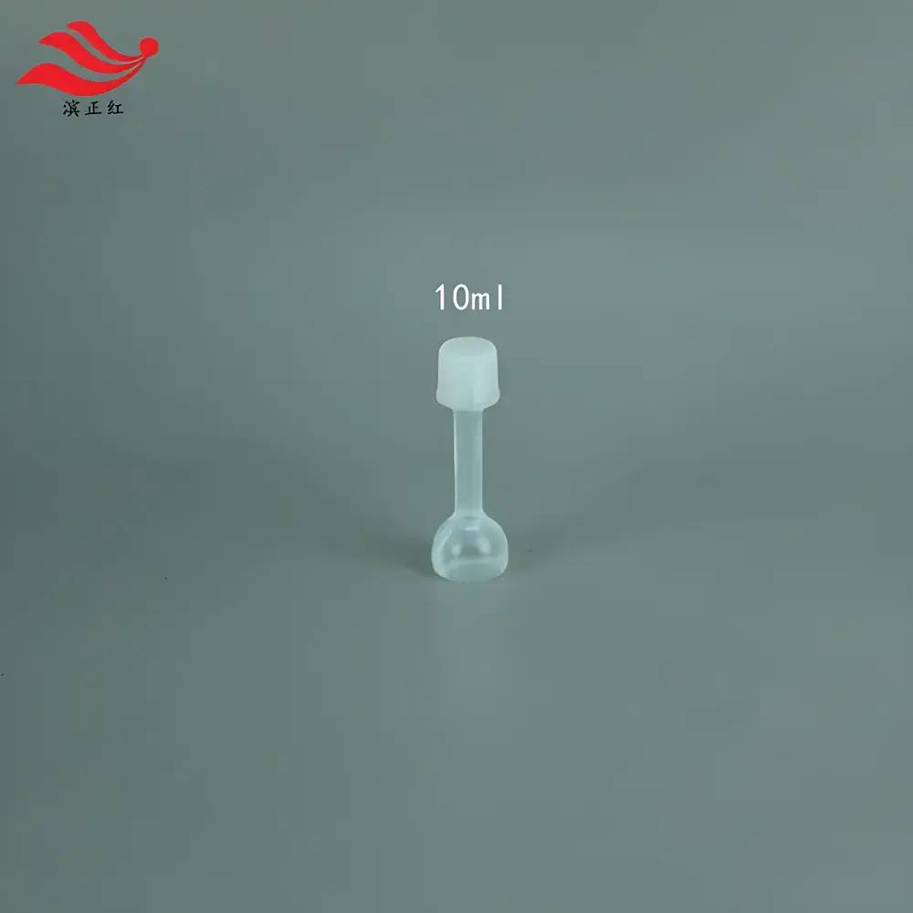
| Brand | Binzhenghong |
|---|---|
| Origin | Jiangsu, China |
| Manufacturer Type | Direct Producer |
| Origin Category | Domestic |
| Grade | Class A |
| Pricing | Available Upon Request |