
Semiconductor Instruments
Filter
Showing 631–660 of 852 results
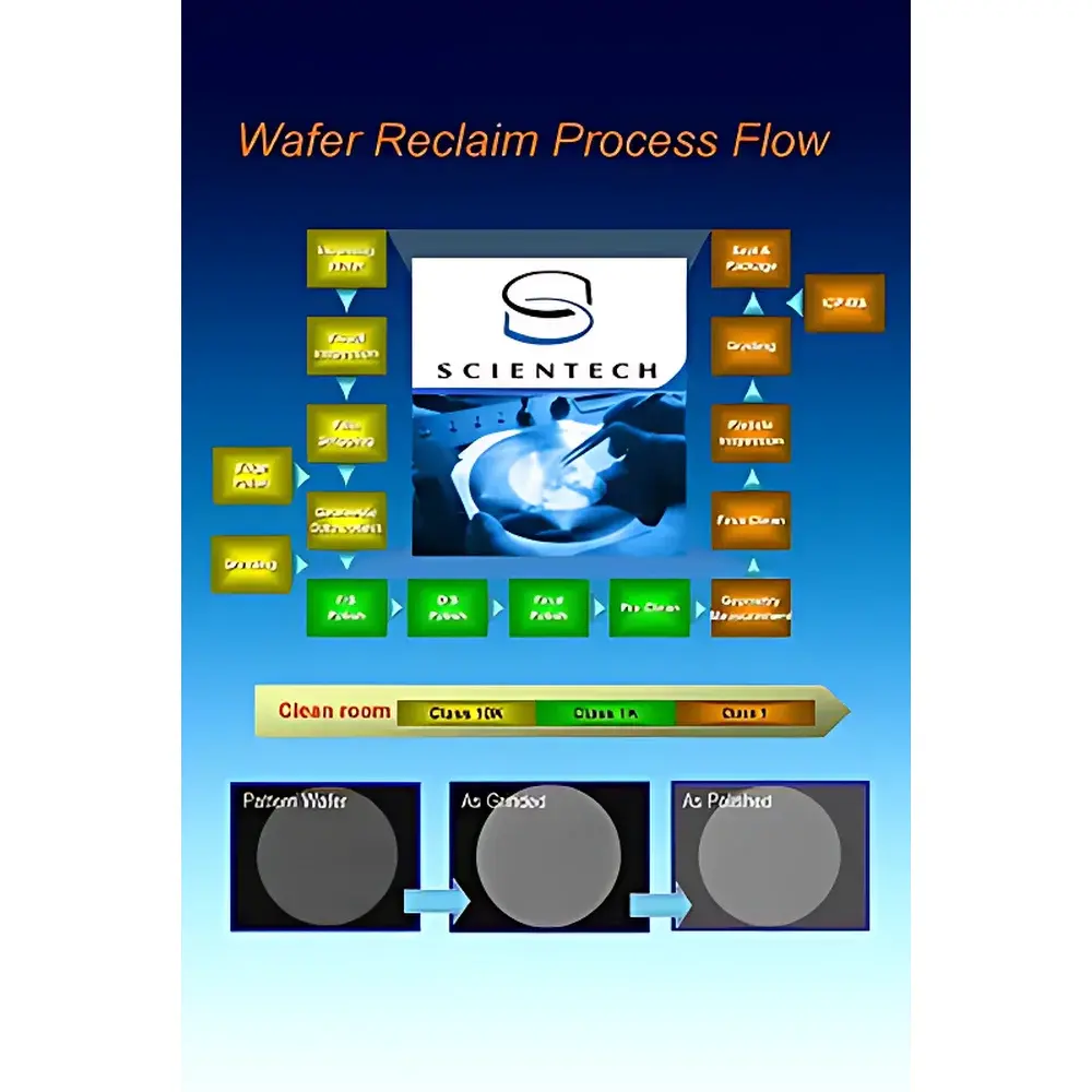
| Brand | Scientech |
|---|---|
| Origin | Taiwan |
| Manufacturer Type | Authorized Distributor |
| Domestic Product Classification | Yes |
| Model | 12-inch |
| Pricing | Available Upon Request |
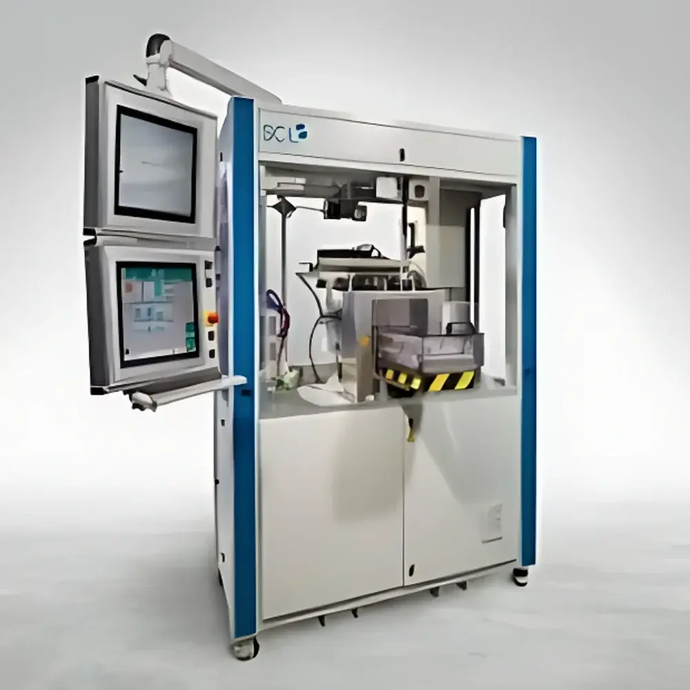
| Brand | SCIL |
|---|---|
| Origin | Netherlands |
| Model | LabSCIL |
| Wafer Size | Up to 8-inch (200 mm) |
| Alignment Accuracy | < 1 µm |
| Imprint Technology | Low-Force Soft-Mold Substrate-Conformal Nanoimprint |
| Compatible Resists | Thermal Sol-Gel, UV Sol-Gel, UV Organic |
| Wafer Thickness Range | 0.3–2.5 mm |
| Footprint (W×L×H) | 1.8 × 1.4 × 2.2 m |
| Resist Application | External Spin-Coater Required |
| Compliance | Designed for ISO Class 5–7 cleanroom integration |
| Software | SCIL Control Suite with Audit Trail & Parameter Logging |
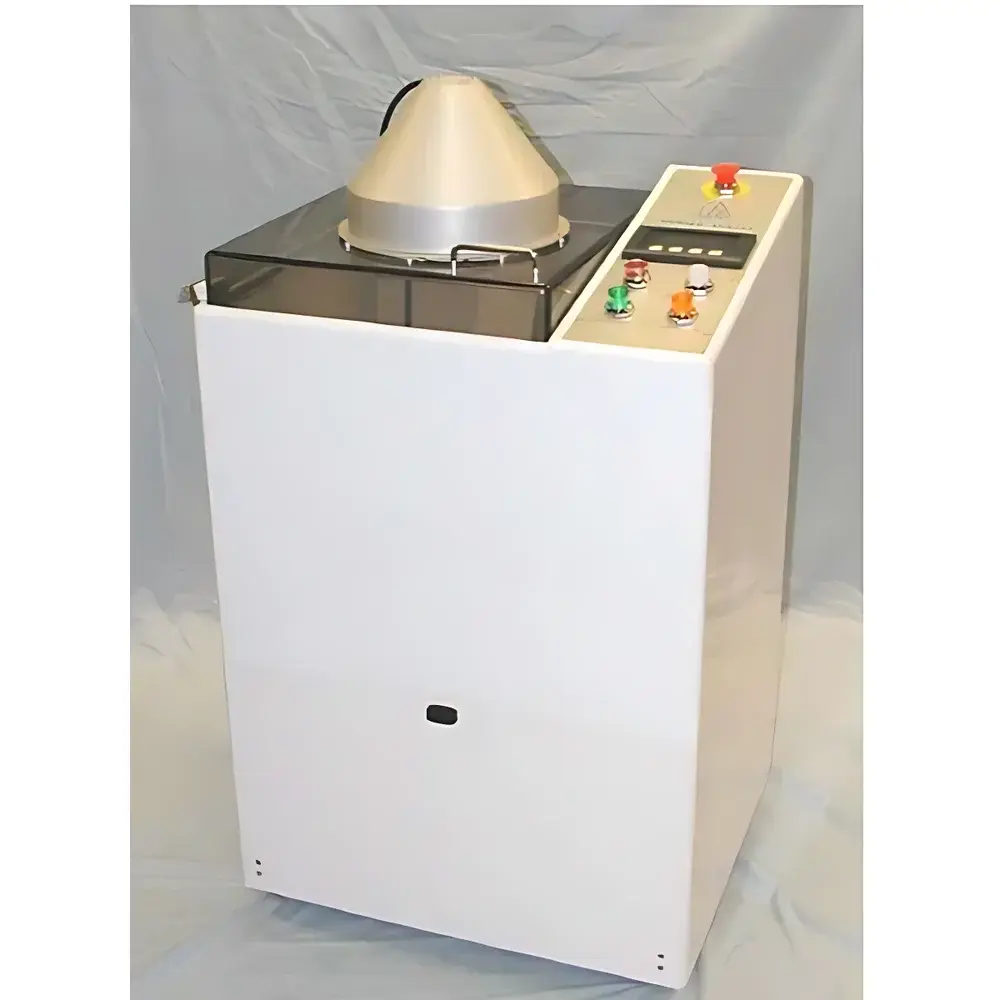
| Origin | USA |
|---|---|
| Manufacturer Type | Authorized Distributor |
| Import Status | Imported |
| Models | SCS112 / SCSe124 / SCSe126 |
| Cleaning Method | Wet Chemical & DI Water-Based Cleaning |
| Equipment Type | Single-Wafer Manual Processing Station |
| Maximum Substrate Diameter | 8 in (SCS112) or 10 in (SCSe124/SCSe126) |
| System Dimensions (W×D×H) | 26 in × 21 in × 40 in |
| Spindle Speed | Up to 2500 rpm |
| Control Architecture | Microprocessor-Based with Touchscreen GUI (SCSe124/SCSe126) or Keypad Interface (SCS112) |
| Preset Recipes | 3 (SCS112) or 10 (SCSe124/SCSe126) |
| Mechanical Arms | 1 (SCS112), 2 (SCSe124), or 4 (SCSe126) |
| Chamber Material | Chemically Resistant Polypropylene |
| Exhaust Configuration | Radial Laminar Flow Chamber (SCSe124/SCSe126) |
| Drying Options | High-velocity N₂ purge, IR heating lamp, or heated DI water rinse |
| Safety Features | Interlocked lid, positive-pressure chamber cover, emergency stop circuitry |
| Power Supply | 220 VAC, 10 A, 50/60 Hz |
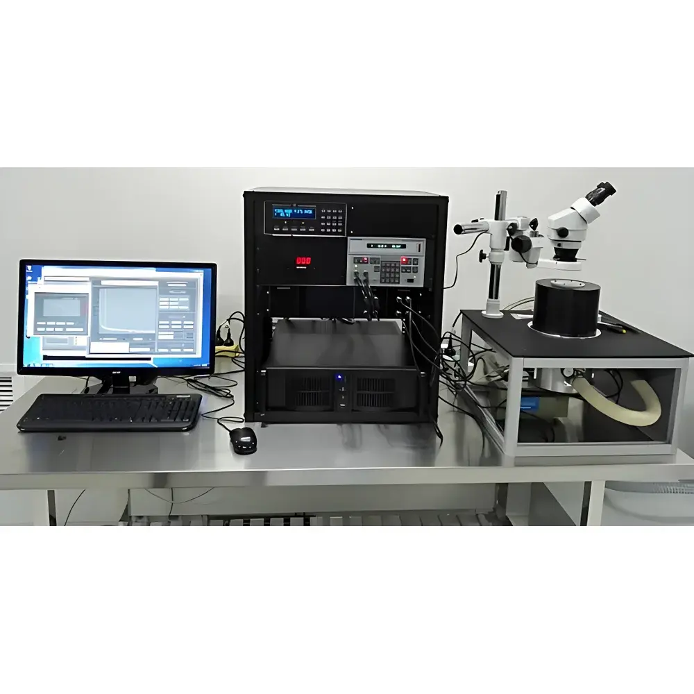
| Brand | Semetrol |
|---|---|
| Origin | USA |
| Model | Semetrol DLTS |
| Temperature Range | 25 K – 700 K |
| Cooling | Closed-Cycle Liquid Helium Refrigerator |
| Capacitance Measurement Frequency | 1 MHz |
| Capacitance Sensitivity | 1 fF |
| Voltage Range | ±100 V (Boonton), ±10 V (DAQ) |
| Voltage Resolution | 0.3 mV (DAQ, <20 V), 1 mV (<20 V), 10 mV (>20 V) |
| Pulse Width Range | 5 μs – >0.1 s (DAQ), 15 ms – >0.1 s (Boonton) |
| Pulse Amplitude | up to 200 V (Boonton), up to 20 V (DAQ) |
| Slew Rate | <20 V/ms (Boonton), 20 V/μs (DAQ) |
| Current Limit | 5 mA |
| Sampling Rate | down to 1 μs |
| Record Length | >10,000 points |
| Time Resolution | 50 ns |
| Capacitance Resolution | <50 aF |
| Automatic Zeroing | Yes |
| Auto-Ranging | Yes |
| Response Time | ~25 μs |
| Compensation Range | 256 pF |
| Test Signal Levels | 15, 30, 50, 100 mV |
| Filtering | Auto-detection and sinusoidal noise suppression |
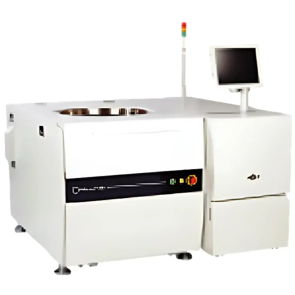
| Brand | SEMICS |
|---|---|
| Origin | South Korea |
| Model | OPUS-SH / OPUS-SD / OPUS3 / OPUS-SS |
| Wafer Compatibility | 6", 8", and 12" (SEMI-compliant) |
| Dimensions (W×D×H) | OPUS-SH: 1490 × 1680 × 960 mm |
| OPUS-SD | 1530 × 1782 × 960 mm |
| XY Travel Range | ±175 mm (SH), ±185 mm × ±175 mm (SD) |
| XY Positioning Accuracy | ±1.5 µm |
| Maximum Downforce | 500 kgf |
| Temperature Range Options | Ambient to +150 °C, -40 °C to +150 °C, -55 °C to +200 °C, and 25 °C environmental chamber control |
| Structural Architecture | Rigid Z-frame with flat-load configuration |
| Key Functionalities | Real-time configuration validation, smart pin alignment algorithm, intelligent probing path optimization, map-shift prevention, drawer-type (SH) or universal probe card interface (SD/OPUS3), full pogo-pin tester compatibility |
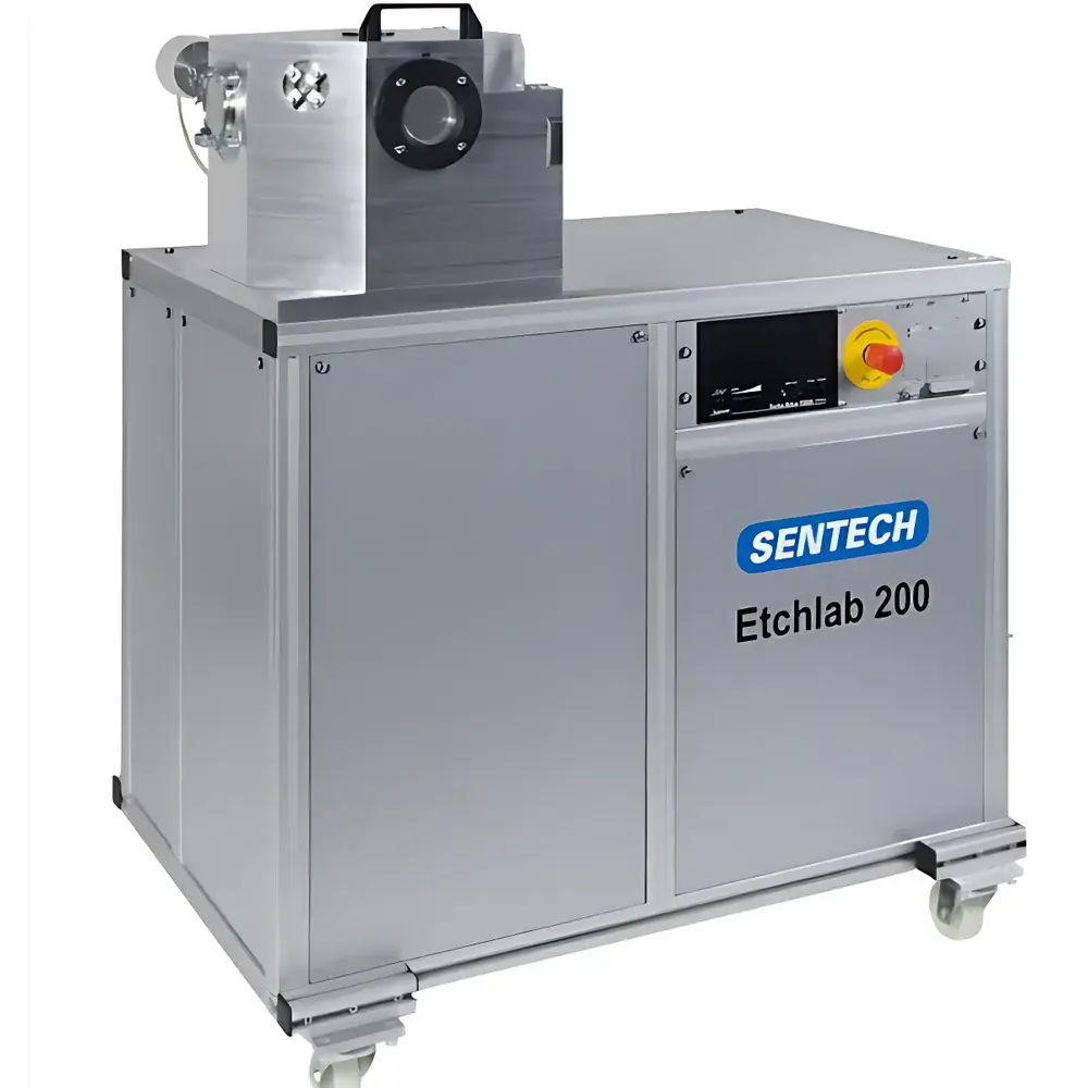
| Brand | SENTECH (Germany) |
|---|---|
| Origin | Germany |
| Model | Etchlab 200 |
| RF Power | 600 W @ 13.56 MHz |
| Vacuum System | 360 L/s Turbo-Molecular Pump + Rotary Vane Backing Pump |
| Wafer Capacity | Up to 200 mm (8-inch) |
| Gas Inlets | 2–12 Configurable Lines |
| Chamber Access | Top-Opening Lid Design |
| Footprint | Compact Benchtop Layout |
| Optional Add-ons | Residual Gas Analyzer (RGA), Optical Emission Spectroscopy (OES), Sample Temperature Control (SLI), High-Vacuum Pressure Monitoring (TP) |
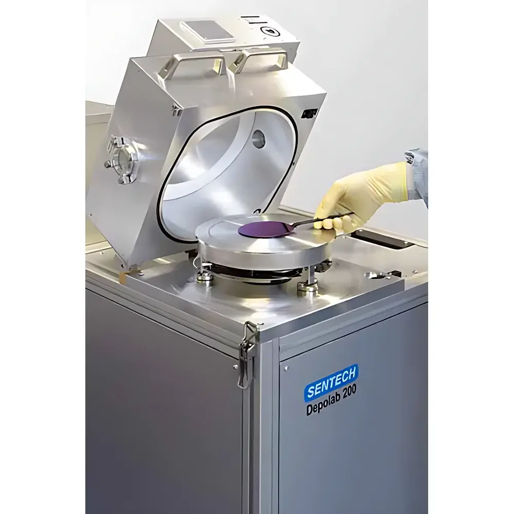
| Origin | Germany |
|---|---|
| Manufacturer Type | Authorized Distributor |
| Origin Category | Imported |
| Model | Etchlab 200 |
| Etching Principle | Equipped with magnetic-field-enhanced Inductively Coupled Plasma (ICP/ISM) or Non-Linear Discharge (NLD) plasma source |
| Etch Rate | Up to 1 µm/min (material and process dependent) |
| Wafer Size Compatibility | 100–200 mm (standard), upgradable to 300 mm |
| Selectivity | Up to 1:20 (e.g., SiO₂:Si) |
| Uniformity | ±5% across wafer |
| Residue Level | <1% (post-etch residue coverage) |
| Aspect Ratio Capability | Up to 1:20 (depth:width) |
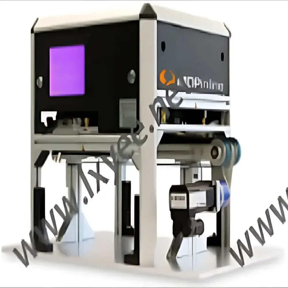
| Brand | SENTECH |
|---|---|
| Origin | Germany |
| Model | MDPinline |
| Application | In-line quantitative minority carrier lifetime mapping of silicon wafers |
| Measurement Principle | Microwave-detected photoconductance decay (µ-PCD) |
| Scan Speed | <1 second per wafer |
| Integration | Conveyor-compatible, no moving mechanical parts |
| Compliance | Designed for semiconductor manufacturing environments compliant with ISO 9001 and SEMI S2/S8 safety standards |
| Software Interface | Ethernet-enabled, supports SECS/GEM protocol for factory automation integration |
| Data Output | Full-wafer lifetime map (pixel-resolved), dual-line resistivity profile, CSV/HDF5 export |
| Calibration | Traceable to NIST-traceable reference wafers |
| Operating Environment | Class 1000 cleanroom compatible (ISO 4), 18–28 °C, <60% RH non-condensing |
| Power Supply | 100–240 V AC, 50/60 Hz, <500 W |
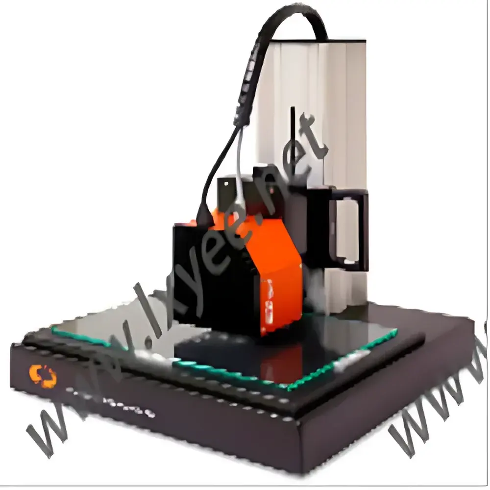
| Brand | SENTECH |
|---|---|
| Origin | Germany |
| Model | MDPspot |
| Type | Contactless, Microwave Photoconductance Decay (μ-PCD) Based Lifetime Tester |
| Sample Handling | Manual Z-axis adjustment (up to 156 mm height) |
| Measurement Mode | Single-point, non-contact, room-temperature operation |
| Material Compatibility | Crystalline and multicrystalline silicon wafers & bricks |
| Compliance | Designed for R&D and process monitoring in PV and semiconductor fabrication environments |
| Software | MDP Control Suite (Windows-based, real-time visualization, CSV export, GLP-compliant data logging) |
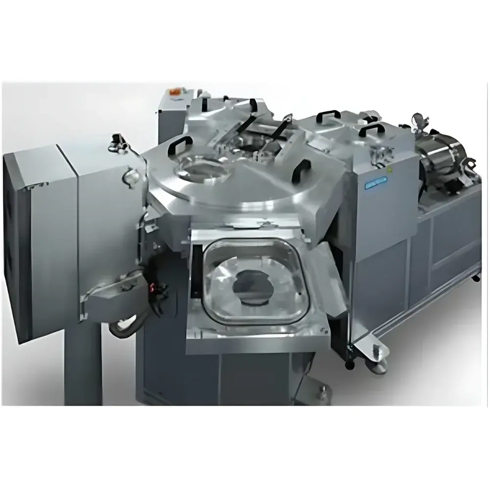
| Brand | SENTECH |
|---|---|
| Origin | Germany |
| Model | SENTECH Multi-Chamber Platform |
| Etching Principle | Capacitively Coupled Plasma (CCP) and/or Inductively Coupled Plasma (ICP) |
| Chamber Configuration | Modular multi-port transfer chamber (3–6 ports) |
| Wafer Handling | Load-lock pre-vacuum chamber and/or vacuum cassette station |
| Maximum Wafer Size | 200 mm |
| Integration Capabilities | ICP etcher, RIE etcher, ALD, PECVD, ICPECVD modules |
| Control Interface | GUI-based process control software compliant with industrial automation standards |
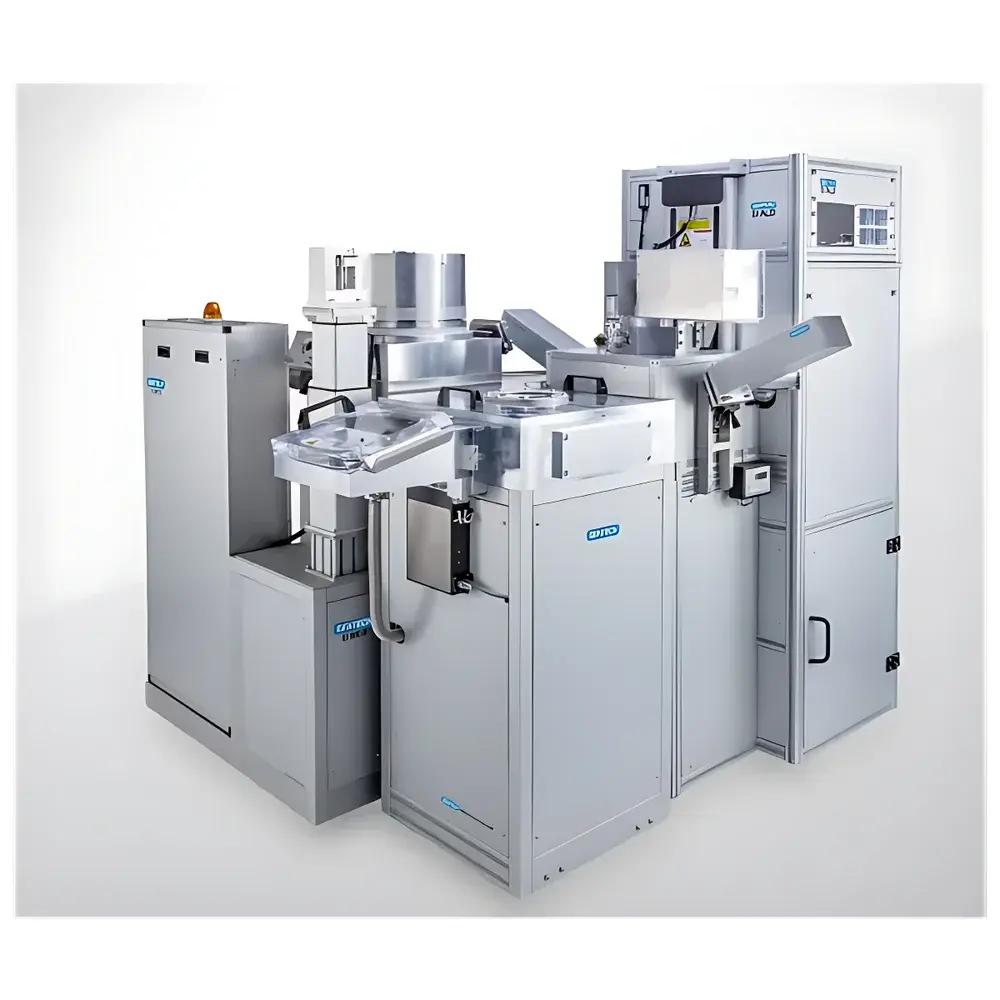
| Brand | SENTECH |
|---|---|
| Origin | Germany |
| Manufacturer Type | Authorized Distributor |
| Origin Category | Imported |
| Model | SENTTECH Cluster System |
| Price | Upon Request |
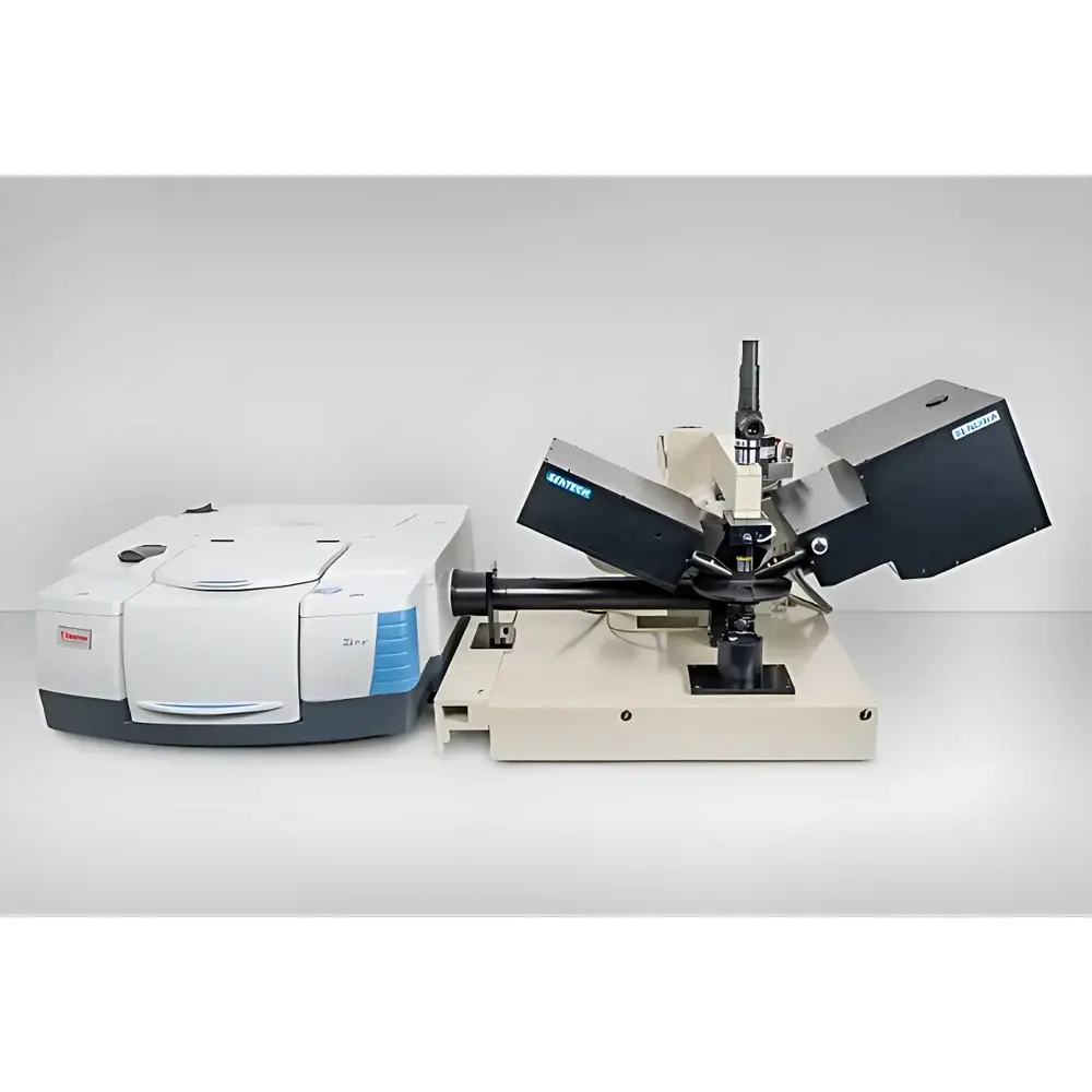
| Brand | SENTECH |
|---|---|
| Origin | Germany |
| Model | SENDIRA |
| Spectral Range | 400–6,000 cm⁻¹ (1.7–25 µm) |
| Detector Options | DTGS or MCT |
| Integrated FTIR Platform | Compatible with Thermo Fisher iS50 |
| Software | SpectraRay/4 + Dedicated FTIR Control Suite |
| Optical Configuration | Purged ellipsometer optics, motorized goniometer, horizontal sample stage, auto-collimating telescope |
| Application Domain | Vibrational spectroscopic ellipsometry for thin-film metrology |
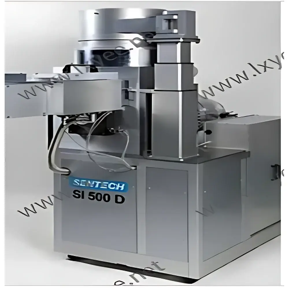
| Brand | SENTECH |
|---|---|
| Origin | Germany |
| Model | SI 500 D |
| Plasma Source | Planar Triple-Spiral Antenna (PTSA) |
| Substrate Temperature Range | RT to +350 °C |
| Vacuum System | Fully Integrated, High-Stability |
| Process Compatibility | SiO₂, SiNₓ, SiONₓ, a-Si, SiC, TEOS-derived films |
| Substrate Size | Up to 200 mm wafers or carrier-mounted substrates |
| Optional Features | Load-lock integration, Laser Endpoint Detection, Substrate Biasing, He-backside Cooling with Real-Time Backside Temperature Sensing |
| Control Architecture | SENTECH Fieldbus-Based SCADA Software with Audit-Trail-Capable UI |
| Compliance Context | Designed for GLP/GMP-aligned R&D and pilot-line fabrication |
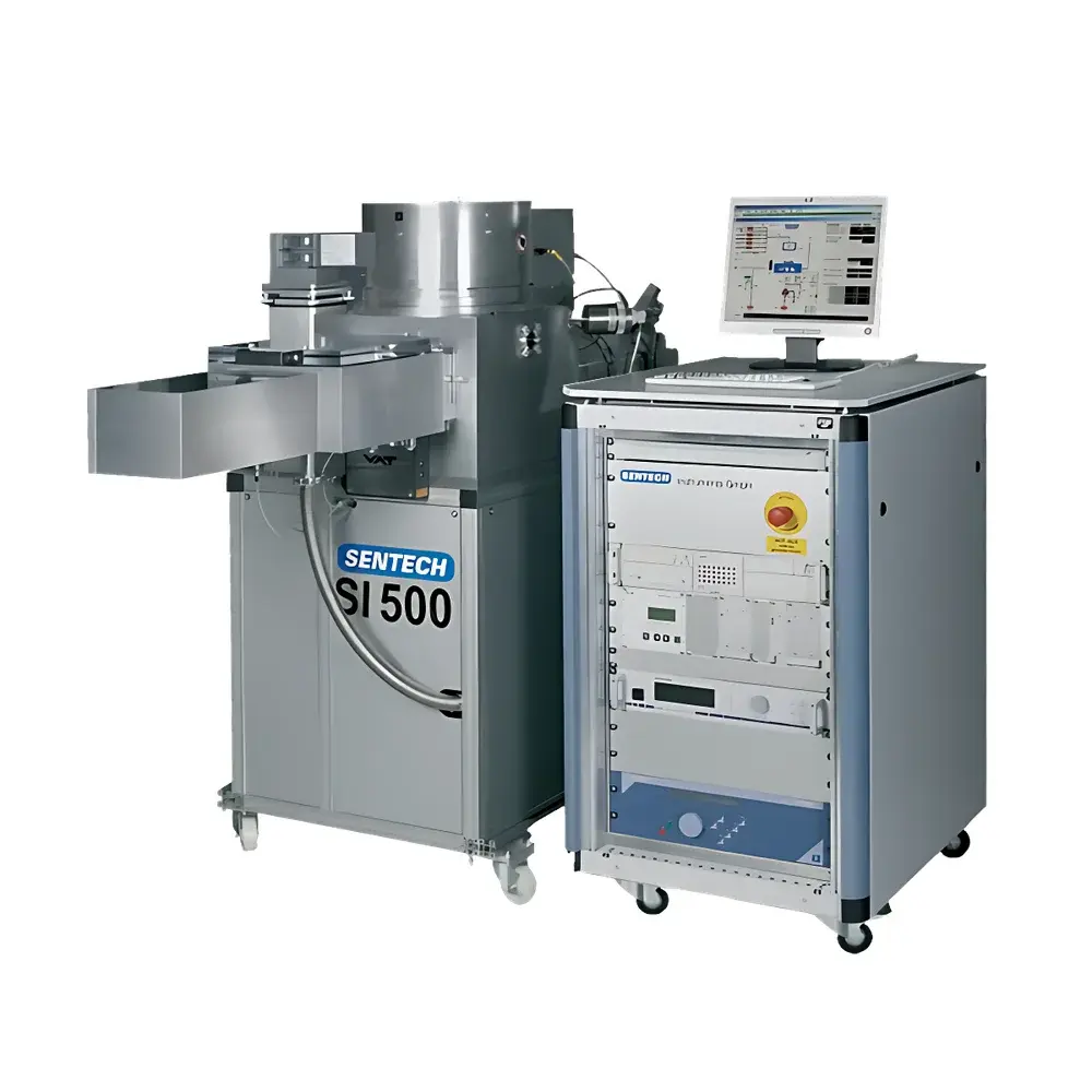
| Origin | Germany |
|---|---|
| Manufacturer Type | Authorized Distributor |
| Origin Category | Imported |
| Model | SI 500 |
| Price | USD 295,000 (FOB Hamburg) |
| RF Source Frequency | 13.56 MHz |
| ICP Power | 1200 W |
| Bias RF Power | 600 W |
| Plasma Source | Planar Triple Spiral Antenna (PTSA) |
| Endpoint Detection | Interferometric In-situ Monitoring |
| Vacuum System | High-throughput Dry Pumping with Independent Gas Flow & Pressure Control |
| Software | SENTECH Advanced Plasma Process Control (APPC) v5.x |
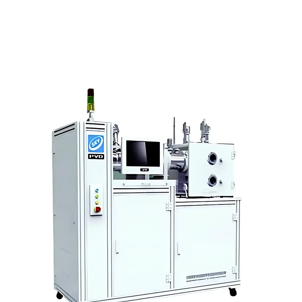
| Brand | Shenyang K.Y. |
|---|---|
| Origin | Liaoning, China |
| Manufacturer Type | Authorized Distributor |
| Country of Origin | China |
| Model | PVD400 |
| Instrument Type | Magnetron Sputtering Coater |
| Application Field | Microelectronics |
| Substrate Size | Ø100 mm (1 × 4-inch wafer) |
| Targets | Three Ø50.8 mm (2-inch) Permanent-Magnet DC/RF Sputtering Targets |
| Maximum Substrate Temperature | 800 °C |
| Thickness Uniformity (within wafer) | ≤ ±3% |
| Base Vacuum | ≤ 6.6 × 10⁻⁵ Pa |
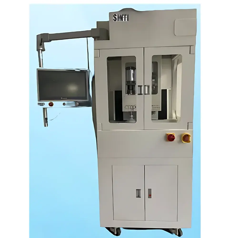
| Brand | SHNTI |
|---|---|
| Origin | Shanghai, China |
| Model | CMP20 |
| Wafer Size | 2", 4", 6" |
| Platen Count | 1 |
| Platen/Head/Conditioner Speed | 0–300 rpm (continuously adjustable) |
| Polishing Head Downforce | 0–4 psi (at 4") |
| Slurry & DI Water Flow | 0–300 mL/min (per channel, peristaltic pump) |
| Stroke Range (Head/Conditioner Reciprocation) | 90 mm |
| Dimensions (L×W×H) | 800 mm × 1000 mm × 2000 mm |
| Optional Modules | Electrochemical Unit (±10 V / ±250 mA, 2-/3-electrode support, CV, etc.), UV Module (λ = 95 nm, 1020 mm × 100 mm emission area, 200 W input power) |
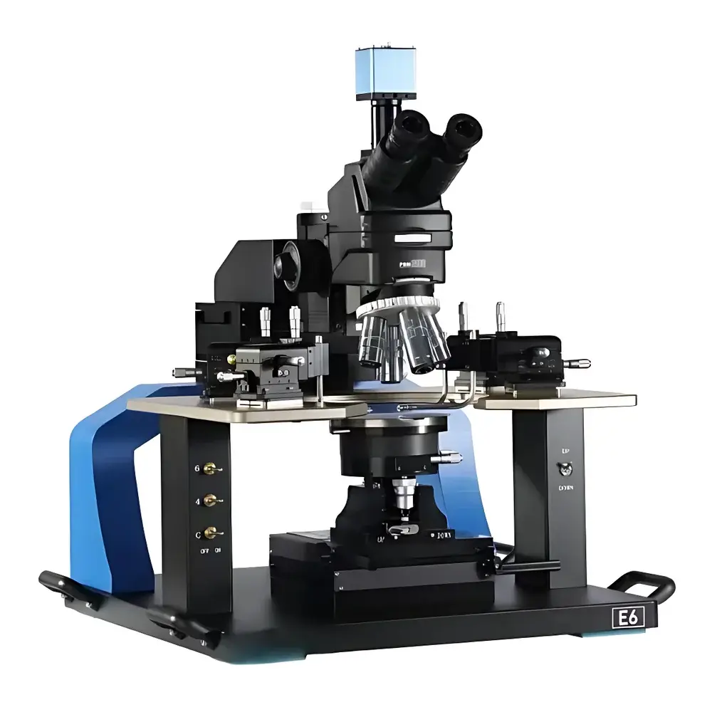
| Brand | SHNTI |
|---|---|
| Origin | Shanghai, China |
| Manufacturer Type | Authorized Distributor |
| Product Category | Surface Resistivity Probe Station |
| Operation Mode | Manual |
| Compatible Wafer Sizes | 4", 6", 8", 12" |
| Modular Expansion Support | mmWave (mmW), Failure Analysis (FA), MEMS, Wafer-Level Reliability (WLR), Optoelectronics |
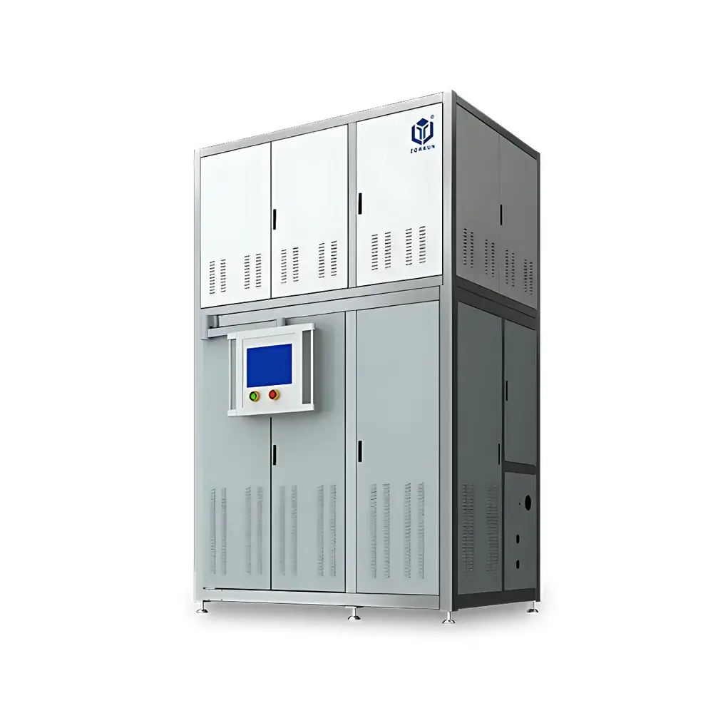
| Brand | SHNTI |
|---|---|
| Origin | Shanghai, China |
| Manufacturer Type | Authorized Distributor |
| Product Category | Domestic |
| Model | IPS Series SiC Crystal Growth System |
| Crystal Types | Silicon Carbide (SiC) only |
| Max. Crystal Diameter | 6-inch and 8-inch |
| Typical Boule Length (Constant-Diameter Section) | 20–30 mm |
| Base Vacuum | ≤5.0 × 10⁻⁵ Pa |
| Pressure Rise Rate | ≤3 Pa / 12 h |
| Microtube Density (6″ P-type Substrate) | <0.5 cm⁻² |
| Resistivity Range (6″ P-type) | 0.015–0.028 Ω·cm |
| Cooling System | Dual-loop water cooling with real-time temperature & flow monitoring |
| Heating Method | Optimized RF induction coil architecture |
| Process Control | Fully integrated PIM self-diagnostic module + multi-stage PID thermal profiling |
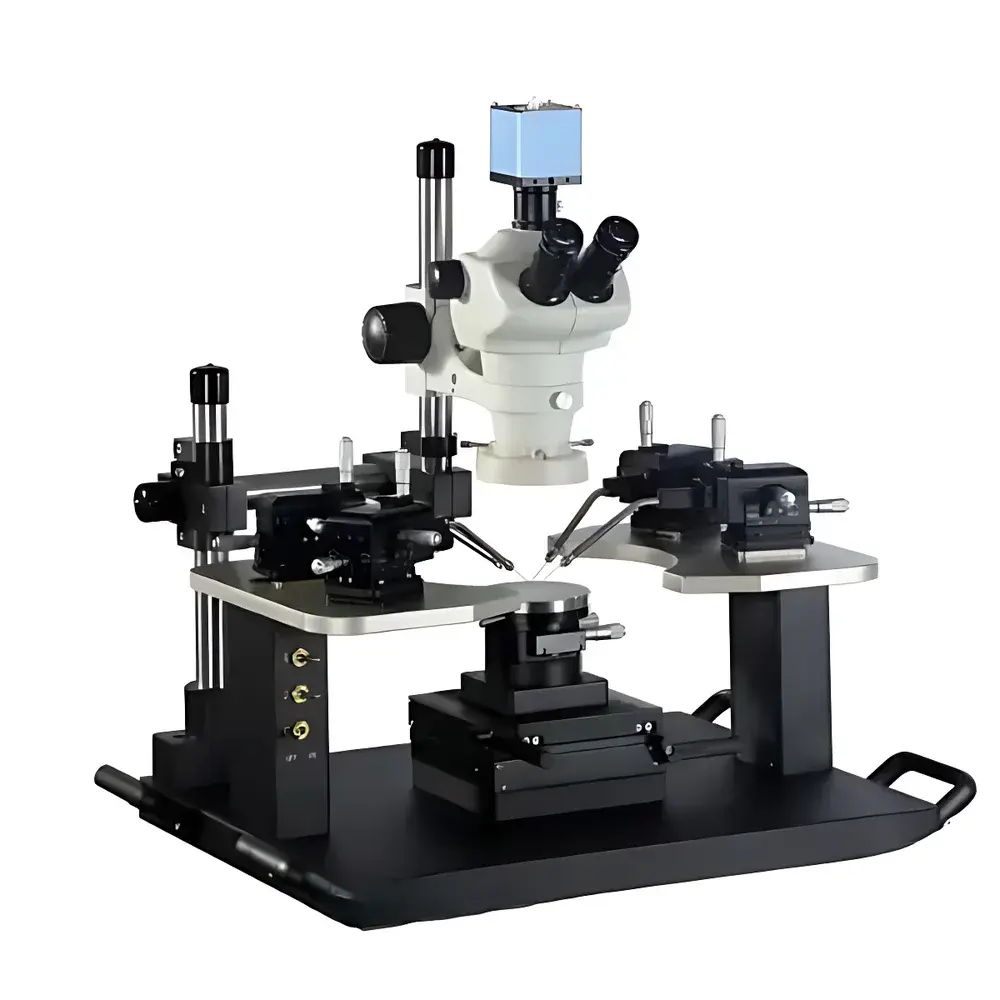
| Brand | SHNTI |
|---|---|
| Origin | Shanghai, China |
| Model | M-Series |
| Operation Type | Manual |
| Maximum Wafer Size | 150 mm (6-inch) and 100 mm (4-inch) |
| Probe Compatibility | DC to 67 GHz RF, MEMS, and Surface Resistivity Measurements |
| Target Pad Size | ≥30 µm |
| Application Scope | Academic Teaching, R&D Lab Characterization, Low-Volume IC Device Evaluation |
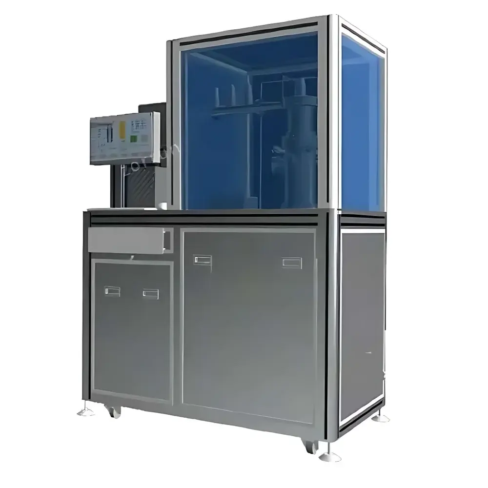
| Brand | SHNTI |
|---|---|
| Origin | Shanghai, China |
| Manufacturer Type | Authorized Distributor |
| Country of Origin | China |
| Model | IMD MPCVD Diamond Growth System |
| Crystal Material | Synthetic Diamond |
| Maximum Crystal Diameter | 2.2 inches (55.9 mm) |
| Typical Crystal Length (Constant-Diameter Zone) | 2–3 cm |
| Process Capability | High-Purity Diamond CVD Deposition, In-situ Thermal Annealing, Homoepitaxial & Heteroepitaxial Growth |
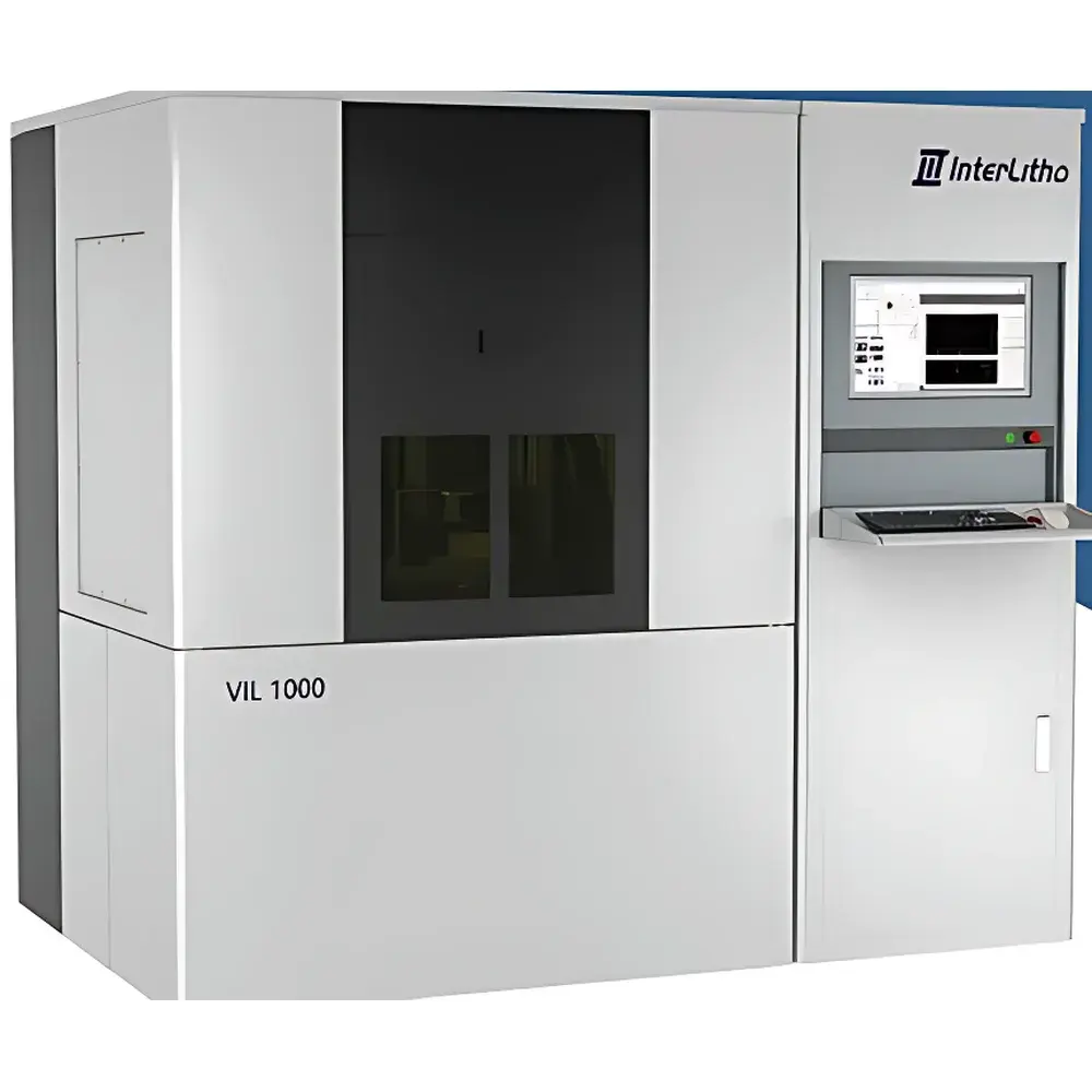
| Brand | SHNTI |
|---|---|
| Origin | Shanghai, China |
| Manufacturer Type | Authorized Distributor |
| Product Origin | Domestic (China) |
| Model | VIL1000 |
| Light Source | Coherent Laser (UV/Deep-UV or Visible, Configurable) |
| Minimum Achievable Line Width | <50 nm |
| Grating Period Range | 240–1500 nm |
| Maximum Exposure Field | 200 mm × 200 mm (8-inch wafer compatible) |
| Pattern Reconfigurability | Real-time, maskless, via beam steering optics |
| Positioning Accuracy | Sub-10 nm (closed-loop piezo stage) |
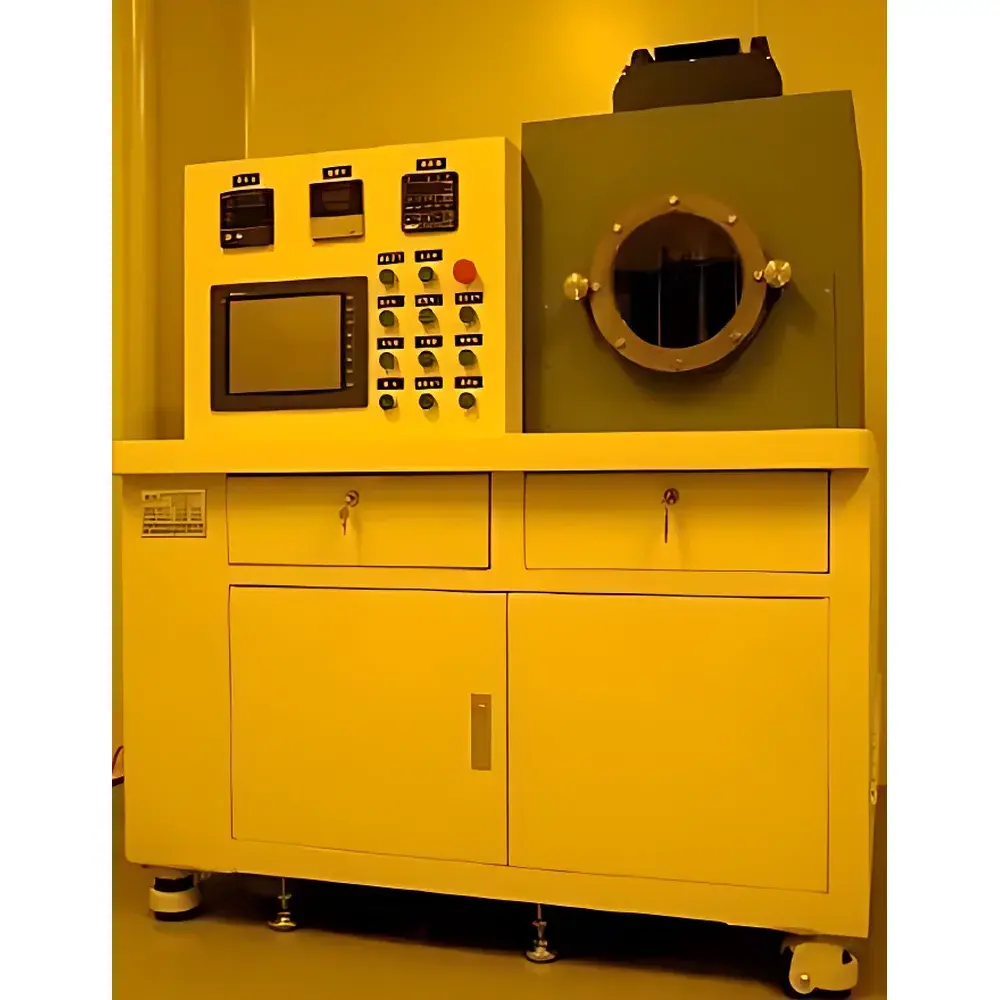
| Brand | SHNTI |
|---|---|
| Origin | Shanghai, China |
| Model | YPL-NIL-SI400 |
| Temperature Range | RT to 350 °C |
| Pressure Range | 0–20 psi (on 4″ wafer) |
| Vacuum Range | 101.3 kPa to 0.1 Pa |
| UV Exposure System | Integrated |
| Sample Holder Max Diameter | 100 mm (4″) |
| Cooling | Integrated Water-Cooled System |
| Control | PLC-based with Touchscreen HMI |
| Software | Proprietary SI400 Machine Control Suite |
| Loading Method | Manual Wafer/Template Handling |
| Sealing | Bellows-Sealed Vacuum Chamber |
| Compliance | Designed for Class 100–1000 cleanroom integration |
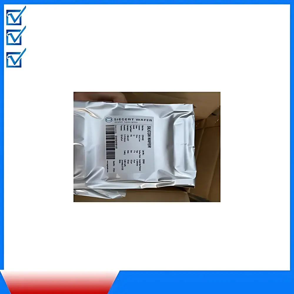
| Brand | Siegert Wafer |
|---|---|
| Origin | Germany |
| Model | Siegert Wafer Series |
| Material Options | Borofloat® 33, Fused Silica |
| Diameter | Up to 200 mm |
| Thickness | 0.5–2.0 mm |
| Shape | Round or Rectangular |
| Surface Coatings | ITO, Photoresist, Custom Thin-Film Layers |
| Compliance | ISO 14644-1 Class 5 Cleanroom Processing |
| Packaging | Vacuum-Sealed, Particle-Free Cassette |
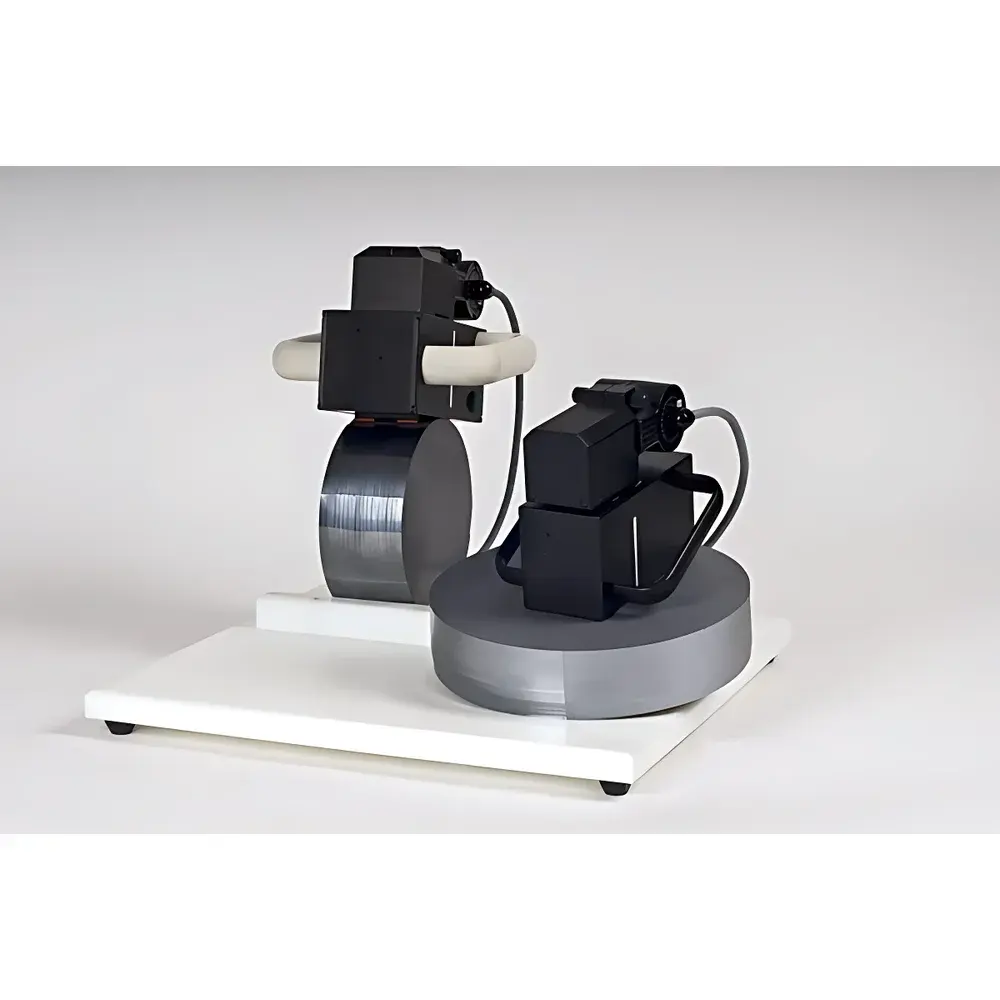
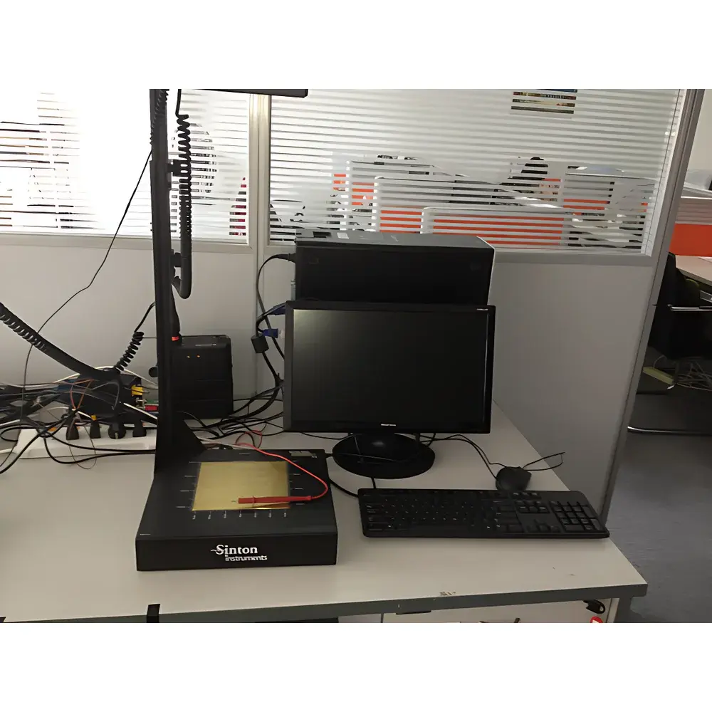
| Brand | Sinton Instruments |
|---|---|
| Origin | USA |
| Model | WCT-120 |
| Minority Carrier Lifetime Range | 0.1 µs – 15 ms |
| Penetration Depth | 3 mm |
| Sample Diameter | up to 210 mm |
| Resistivity Measurement Range | 0.15 – 300 Ω·cm |
| Test Material | Silicon Wafers |
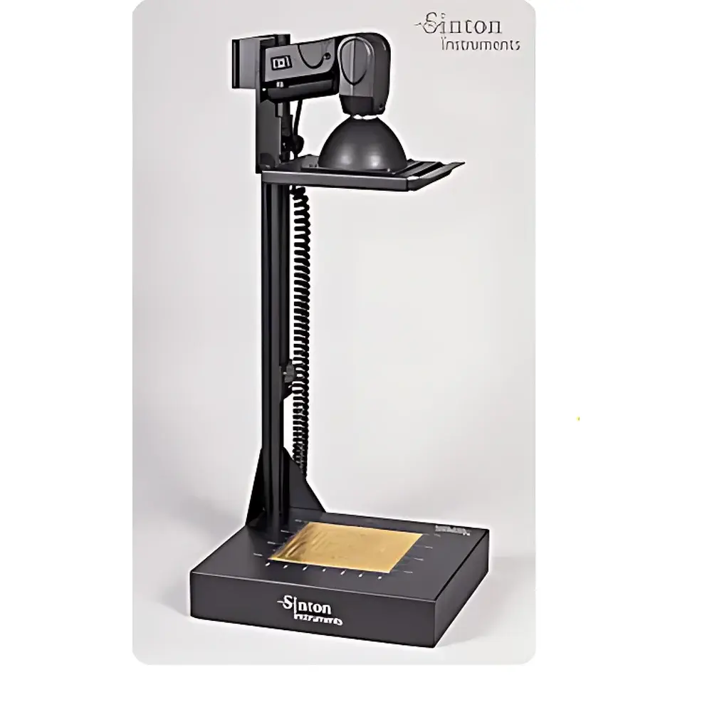
| Brand | Sinton Instruments |
|---|---|
| Origin | USA |
| Model | WCT-120MX + Suns-VocMX |
| Minority Carrier Lifetime Range | 0.1 µs – 15 ms |
| Penetration Depth | 3 mm |
| Sample Diameter | Up to 230 mm |
| Resistivity Range | 0.15 – 300 Ω·cm |
| Material Compatibility | Silicon wafers |
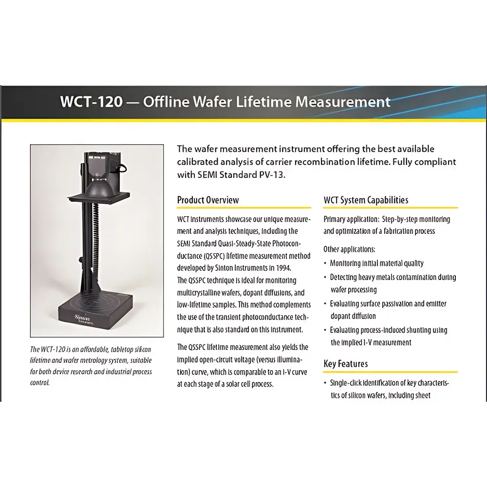
| Brand | Sinton Instruments |
|---|---|
| Origin | USA |
| Model | WCT-120MX + Suns-VocMX |
| Minority Carrier Lifetime Range | 0.1 µs – 15 ms |
| Penetration Depth | 3 mm |
| Maximum Sample Diameter | 230 mm |
| Resistivity Range | 0.15 – 300 Ω·cm |
| Compatible Material | Silicon wafers |
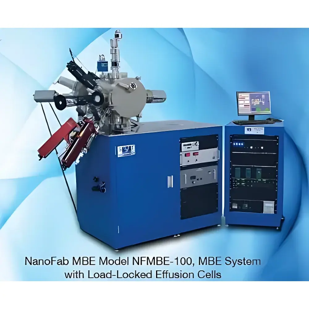
| Origin | USA |
|---|---|
| Manufacturer Type | Authorized Distributor |
| Origin Category | Imported |
| Model | SMART NanoFab |
| Pricing | Upon Request |
| Source Capacity | 4 or 8 effusion cells / e-beam sources |
| Integrated In-situ Monitors | RHEED, QCM, Linear Beam Flux Monitor |
| Growth Modes | Thermal Evaporation, E-beam Evaporation, RF Plasma, Pulsed Laser Deposition (PLD), Sputtering, Gas-Phase Precursor Delivery |
| Compatible Materials | III–V (e.g., GaAs, InP), II–VI (e.g., CdTe, ZnSe), II–Oxides (e.g., ZnO), III–Nitrides (e.g., GaN, AlN), and other compound semiconductors |
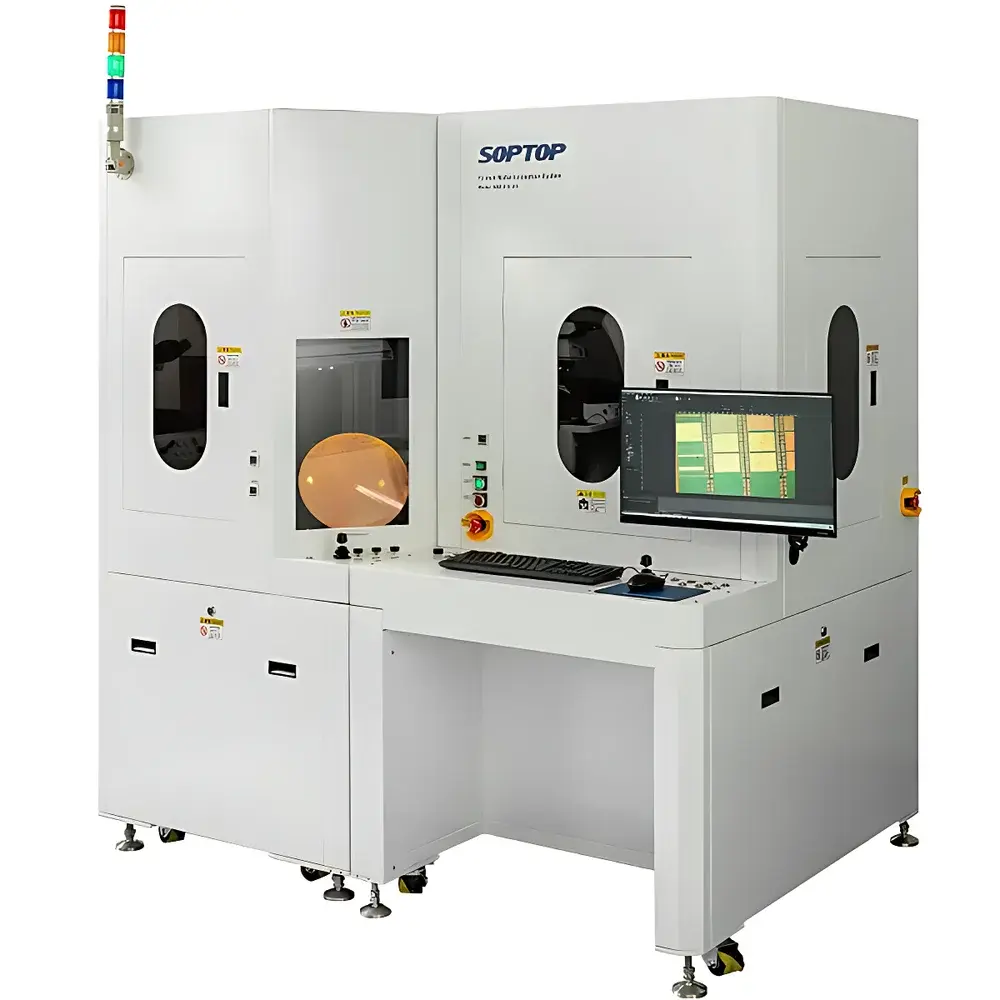
| Brand | SOPTOP |
|---|---|
| Origin | Zhejiang, China |
| Manufacturer Type | Original Equipment Manufacturer (OEM) |
| Regional Classification | Domestic (China) |
| Model | AWL Series |
| Pricing | Upon Request |
| Primary Applications | Front-end & back-end wafer process monitoring, outgoing wafer quality control |
| Supported Wafer Diameters | 100 mm, 150 mm, 200 mm, 300 mm |
| Configurations | AWL046 (4″/6″), AWL068 (6″/8″), AWL812 (8″/12″) |
| Macro Inspection | 360° full-rotation stage with dual-side tilt (front-side max 70°, back-side 1 max 90°, back-side 2 max 160°) |
| Micro Inspection | Semi-apochromatic metallurgical objectives supporting brightfield, darkfield, DIC, and polarized light modes |
| Vacuum Chuck | Manual quick-release mechanism |
| Control System | Motorized precision stage with μm-level defect resolution |

| Brand | SENTECH |
|---|---|
| Origin | Germany |
| Model | SpectraRay/4 |
| Software Type | Spectroscopic Ellipsometry Data Acquisition, Modeling & Analysis Platform |
| Material Database | Integrated Comprehensive Library (Oxides, Nitrides, Metals, Polymers, Amorphous Si, Organic Layers, etc.) |
| Dispersion Models | Cauchy, Tauc-Lorentz, Cody-Lorentz, Drude, Sellmeier, B-Spline, User-Defined Custom Models |
| Mapping Capabilities | 2D Color/Contour/Deviation/3D Surface Plots, Statistical Summary (Mean, Std Dev, Min/Max, Histograms) |
| Simulation Engine | Wavelength-, Angle-, Energy-, Temperature-, Time-Dependent Optical Response Modeling |
| Reporting | Export to Microsoft Word (*.doc), Full Experiment Archiving (Raw Data, Model Definitions, Fitting Logs, Annotations) |
| Scripting | Python-based Automation Interface for Hardware Control (Stages, Heaters, Cryostats, Environmental Chambers) |
| Compliance Support | Audit Trail Logging, User Access Levels, Electronic Signature Ready (FDA 21 CFR Part 11–ready architecture) |