
Semiconductor Instruments
Filter
Showing 511–540 of 852 results
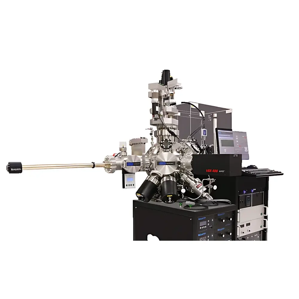
| Brand | Neocera |
|---|---|
| Origin | USA |
| Model | Pioneer 180 Laser MBE/PLD System |
| Substrate Heating | 1000 °C (laser heater), 850 °C (radiant heater) |
| Substrate Size | 1 cm × 1 cm (laser-heated stage), 2″ diameter (radiant-heated stage) |
| Vacuum Chamber Diameter | 18″ |
| RHEED Gun Voltage | 30 keV |
| RHEED Operating Pressure | ≤500 mTorr (O₂) |
| Gas Flow Control | O₂/N₂ up to 100 SCCM |
| Software Platform | Windows 7 + LabVIEW 2013 |
| Target Mounting Options | 6 × 1″ or 3 × 2″ rotating target holder |
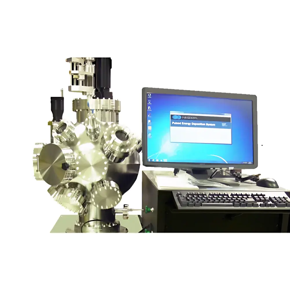
| Brand | Neocera |
|---|---|
| Origin | USA |
| Model | Pioneer 180 MAPLE PLD System |
| Substrate Heating | Up to 500 °C with programmable controller |
| Substrate Size | Max. 2" diameter or multiple 1 cm × 1 cm samples |
| Substrate Rotation | 20 RPM |
| Vacuum Chamber Diameter | 18" |
| Target Stage | LN₂-cooled, single-target standard (multi-target optional) |
| Gas Flow Control | 50–100 SCCM MFC |
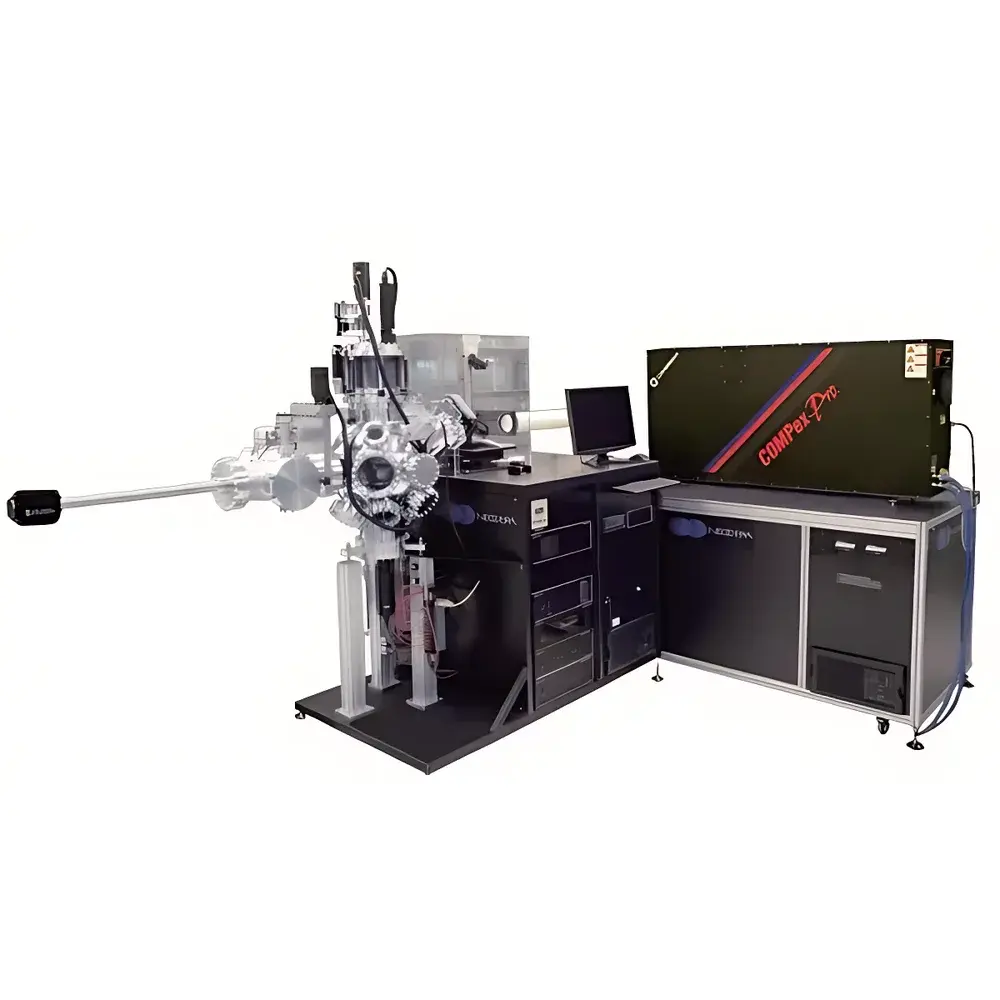
| Brand | Neocera |
|---|---|
| Origin | USA |
| Model | Pioneer 180 PLD System |
| Vacuum Base Pressure | ≤5×10⁻⁹ Torr |
| Chamber Diameter | 18 in |
| Max Substrate Size | 6 in |
| Max Target Capacity | 6×1″ or 3×2″ |
| Substrate Heater | Radiant, O₂-compatible up to 1 atm (760 Torr) |
| Max Substrate Temperature | 850 °C (upgradable to 1000 °C) |
| Turbo Pump Speed | 400 L/s (software-controlled) |
| In-situ Diagnostics Support | RHEED, LAXS, IES |
| Load-Lock Compatible | Yes |
| Multi-Source Integration Options | PED, RF/DC Sputtering, DC Ion Gun |
| UHV Cluster Integration Ready | XPS, ARPES, MBE |
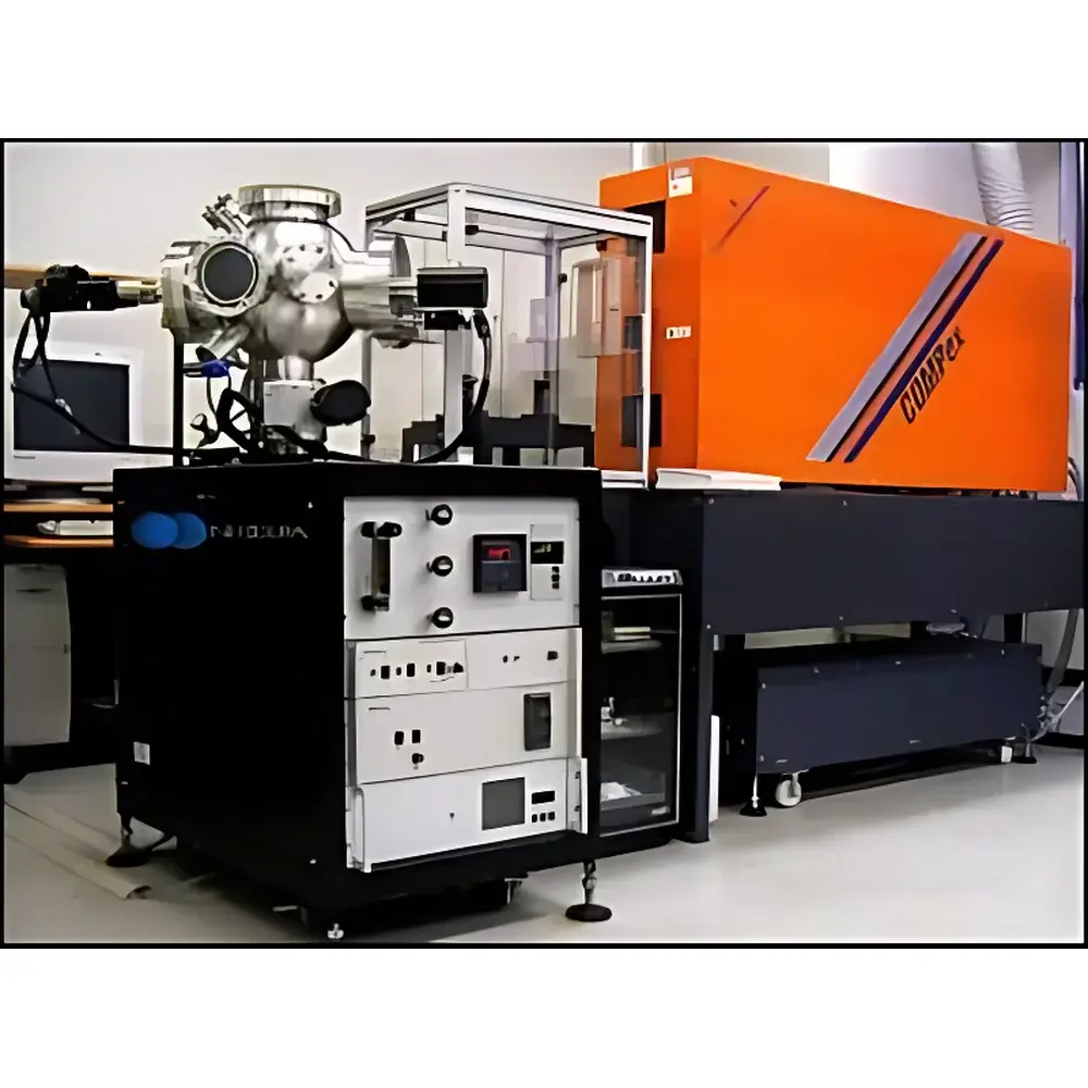
| Origin | USA |
|---|---|
| Manufacturer Type | Authorized Distributor |
| Origin Category | Imported |
| Model | PLD |
| Pricing | Available Upon Request |
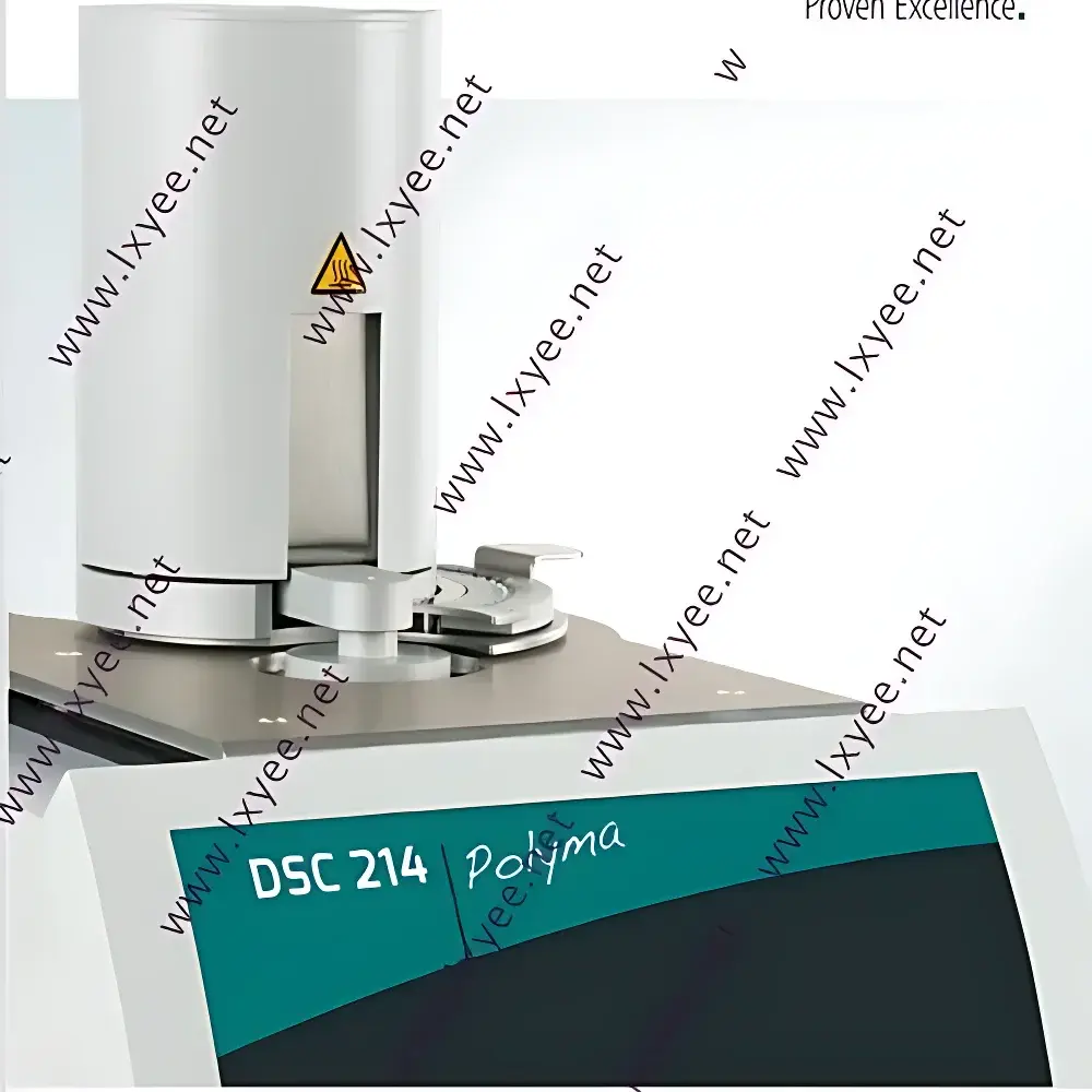
| Brand | Netzsch |
|---|---|
| Origin | Germany |
| Model | DSC 214 Polyma |
| Temperature Range | −100 °C to 600 °C |
| Heating/Cooling Rate | up to 500 °C/min |
| Sensor Type | Corona® high-reproducibility heat-flux sensor |
| Crucible System | Concavus® concave-bottom crucibles with fixed annular contact geometry |
| Software Platform | Proteus® with Smart Mode, Expert Mode, TM-DSC, Beflat® baseline correction, Auto-Analysis, Identify™ polymer recognition database |
| Compliance | ISO 11357-1, ASTM E794, ASTM E1356, USP <1151>, GLP/GMP-ready audit trail (FDA 21 CFR Part 11 optional) |
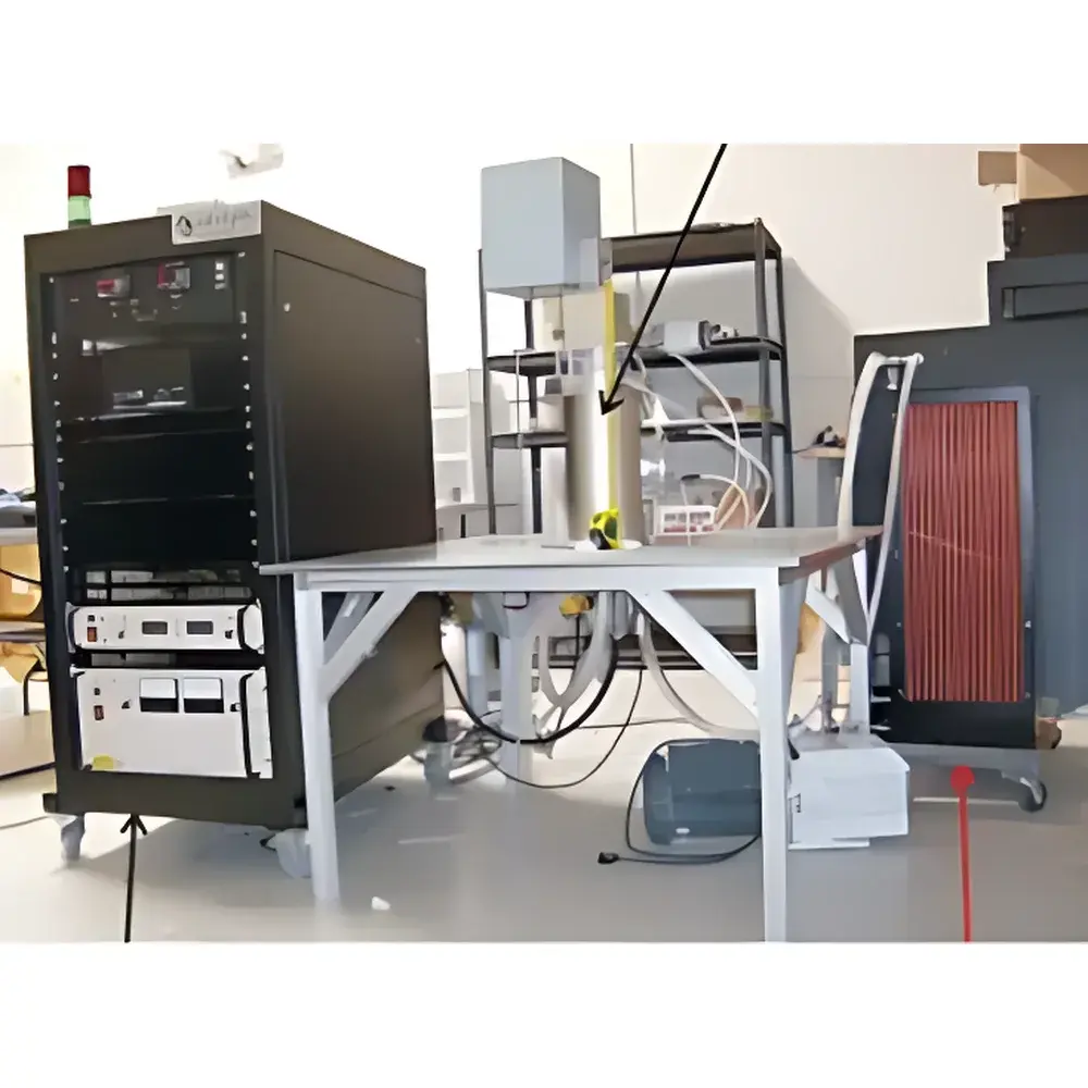
| Origin | USA |
|---|---|
| Manufacturer Type | Distributor |
| Origin Category | Imported |
| Model | DD110M110 |
| Pricing | Upon Request |
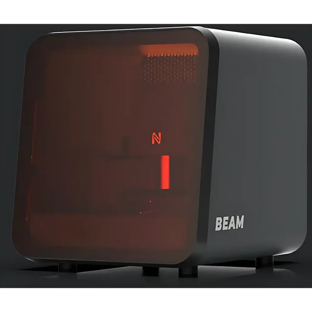
| Brand | NILT |
|---|---|
| Origin | Denmark |
| Manufacturer Type | Authorized Distributor |
| Origin Category | Imported |
| Model | BEAM |
| Exposure Mode | Proximity-style Direct Write |
| Resolution | ≤500 nm (line width) |
| Light Source | UV Diode Lasers |
| Wavelengths | 365 nm, 385 nm, 405 nm |
| Illumination Uniformity | Optimized via Dynamic Beam Shaping & Real-time Power Calibration |
| Exposure Field | 106 mm × 106 mm or 150 mm × 150 mm (tileable) |
| Autofocus Speed | <1 s (piezo-driven closed-loop Z-control) |
| Pattern Writing Speed | <2 s per 10 mm × 10 mm field (at 500 nm resolution, AZ5214E resist) |
| Maximum Substrate Size | 6-inch (150 mm) wafers or square substrates up to 150 mm × 150 mm |
| Alignment Accuracy | <±200 nm (multi-layer, vision-based auto-alignment) |
| Software Interface | GDSII-native workflow with real-time pattern preview, tile stitching, and wafer-level navigation |
| Brand | NILT |
|---|---|
| Origin | Imported |
| Manufacturer Type | Authorized Distributor |
| Exposure Mode | Proximity |
| Resolution | 500 nm |
| Light Source | UV Laser |
| Wavelengths | 405 nm, 365 nm, 385 nm |
| Illumination Uniformity | Direct-write scanning mode |
| Maximum Exposure Area | 150 mm × 150 mm |
| Compatible Substrate Sizes | Up to 6-inch wafers |
| Autofocus Speed | <1 s (piezo-driven closed-loop optical focus control) |
| Pattern Writing Speed | <2 s per defined exposure field |
| Alignment Method | Semi-automated multi-layer alignment with real-time image recognition |
| Software Interface | GDSII-compatible, CNC-style navigation (WASD), on-the-fly pattern placement, wafer-level map visualization |
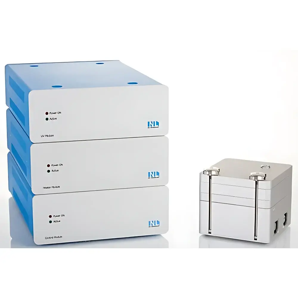
| Brand | NILT |
|---|---|
| Origin | Denmark |
| Manufacturer Type | Authorized Distributor |
| Origin Category | Imported |
| Model | CN1 |
| Price Range | USD 7,000 – 14,000 (FOB Copenhagen) |
| Minimum Feature Size | 20 nm |
| Thermal Imprint Temperature | 200 °C (upgradable to 240 °C) |
| UV Wavelength | 365 nm |
| Pressure Range | 0.3–11 bar |
| Vacuum Level | down to 0.1 mbar |
| Substrate/Template Max Diameter | 100 mm (4-inch), upgradable to 200 mm (8-inch) |
| Control | Fully computer-programmed, GUI-driven operation |
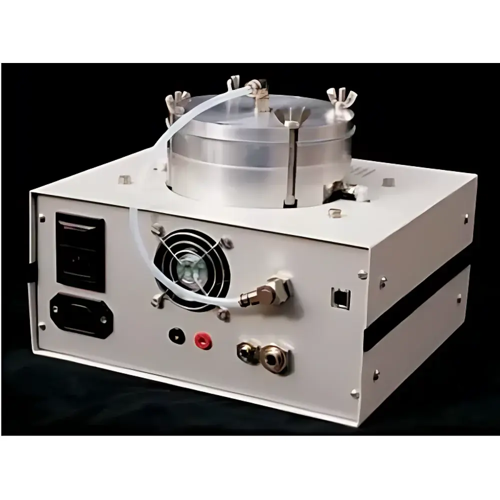
| Brand | NILT |
|---|---|
| Origin | Imported |
| Manufacturer Type | Authorized Distributor |
| Model | CNI |
| Price Range | USD 42,000–70,000 (FOB) |
| Minimum Feature Size | <20 nm |
| Imprint Area Compatibility | 2-inch to 4-inch wafers (customizable) |
| Heating/Cooling Rate | Rapid thermal cycling (<60 s ramp-up/down) |
| Vacuum Requirement | 0.4–0.8 bar (vacuum flow ≥1 mL/min) |
| Pneumatic Supply | Compressed air or N₂ at 6–10 bar |
| Electrical Input | 110–240 V AC, 50–60 Hz, ≥200 W |
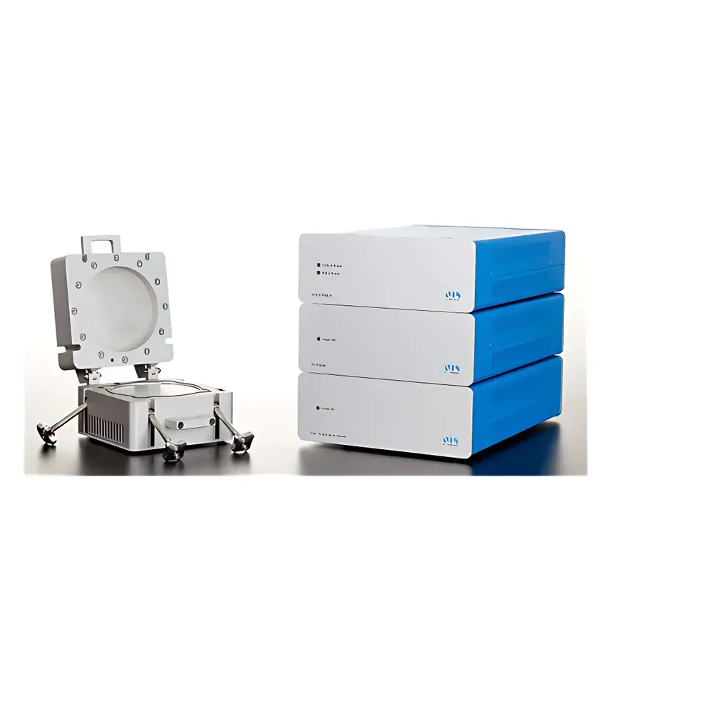
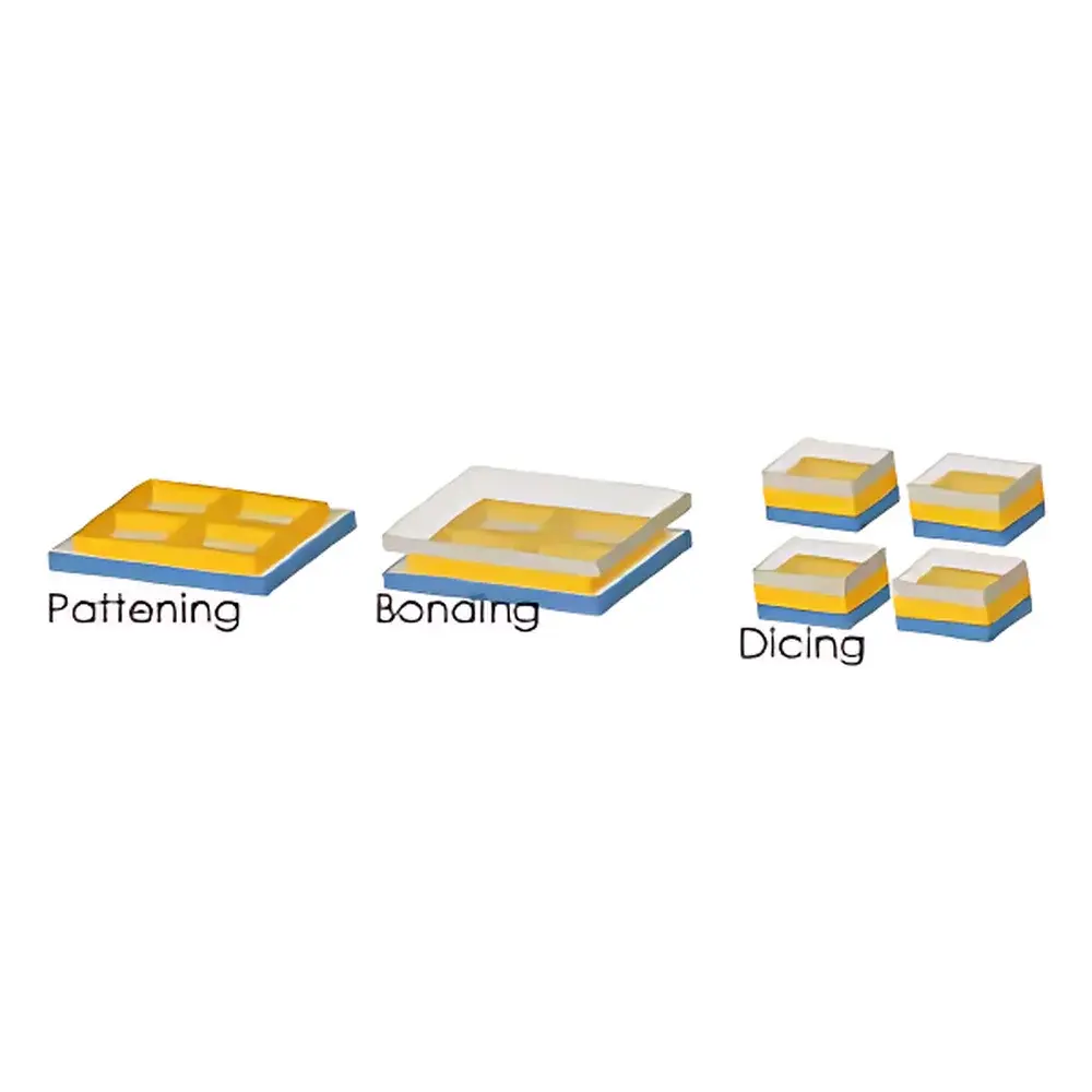
| Brand | NILT |
|---|---|
| Origin | Denmark |
| Manufacturer Type | Authorized Distributor |
| Origin Category | Imported |
| Model | CNI V4.0 PV |
| Pricing | Upon Request |
| Imprint Area | Up to Ø210 mm (8″) |
| Chamber Height | 20 mm |
| Thermal NIL Max Temp | 200 °C (optional 250 °C module) |
| UV-NIL Wavelength | 365 nm (optional 405 nm module) |
| Vacuum Level | ≤0.1 mbar |
| Maximum Imprint Pressure | 11 bar |
| Control Interface | Laptop-based with dedicated software |
| Automation Level | Fully automated process execution (manual stamp/substrate loading) |
| Form Factor | Benchtop, modular, plug-and-play |
| Brand | NIPPON FILCON |
|---|---|
| Origin | Japan |
| Manufacturer Type | Authorized Distributor |
| Origin Category | Imported |
| Model | NIPPON KAYAKU KPM-500 DFR |
| Pricing | Upon Request |
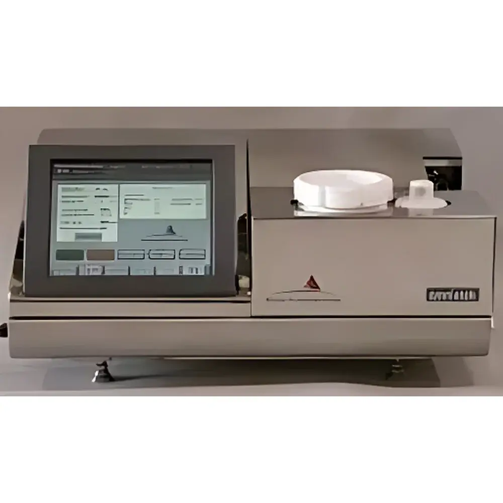
| Brand | Nisene |
|---|---|
| Origin | USA |
| Manufacturer Type | Authorized Distributor |
| Product Category | Imported |
| Model | OmniEtch |
| Pricing | Available Upon Request |
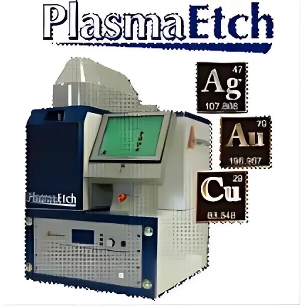
| Brand | Nisene |
|---|---|
| Origin | USA |
| Model | PlasmaEtch |
| Technology | Microwave-induced plasma etching |
| Patent | US Patent 9,548,227 B2 |
| Compliance | RoHS-compliant process, halogen-free etchant chemistry |
| Application | Semiconductor IC decapsulation for failure analysis (FA), cross-sectioning, and package-level defect inspection |
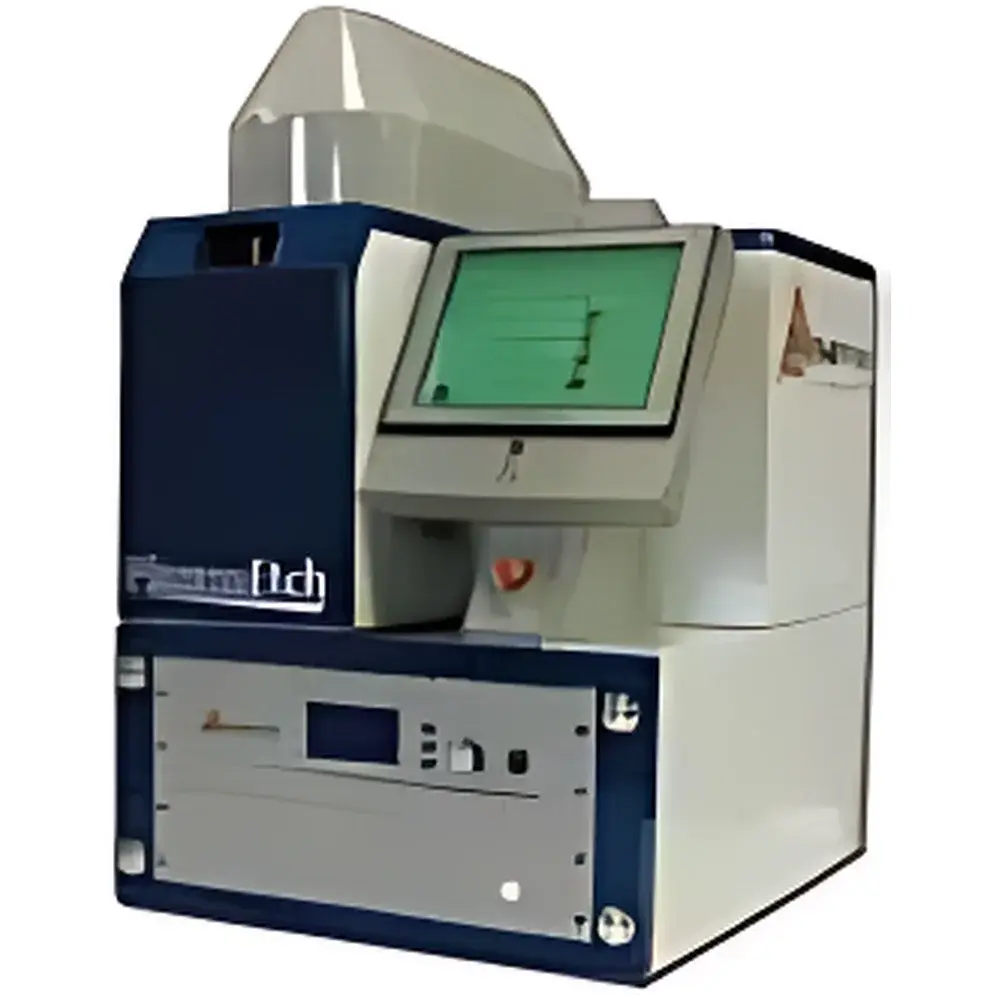
| Brand | Nisene |
|---|---|
| Origin | USA |
| Manufacturer Type | Authorized Distributor |
| Origin Category | Imported |
| Model | PlasmaEtch |
| Pricing | Available Upon Request |
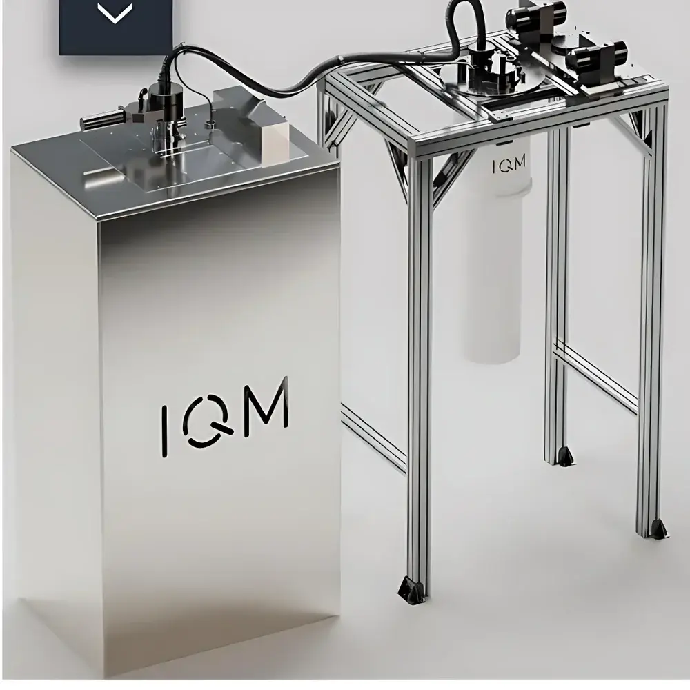
| Brand | 1124123/13213112 |
|---|---|
| Origin | France |
| Supplier Type | Authorized Distributor |
| Import Status | Imported |
| Model | NISQ-5 |
| Price | USD 1.4M (FOB) |
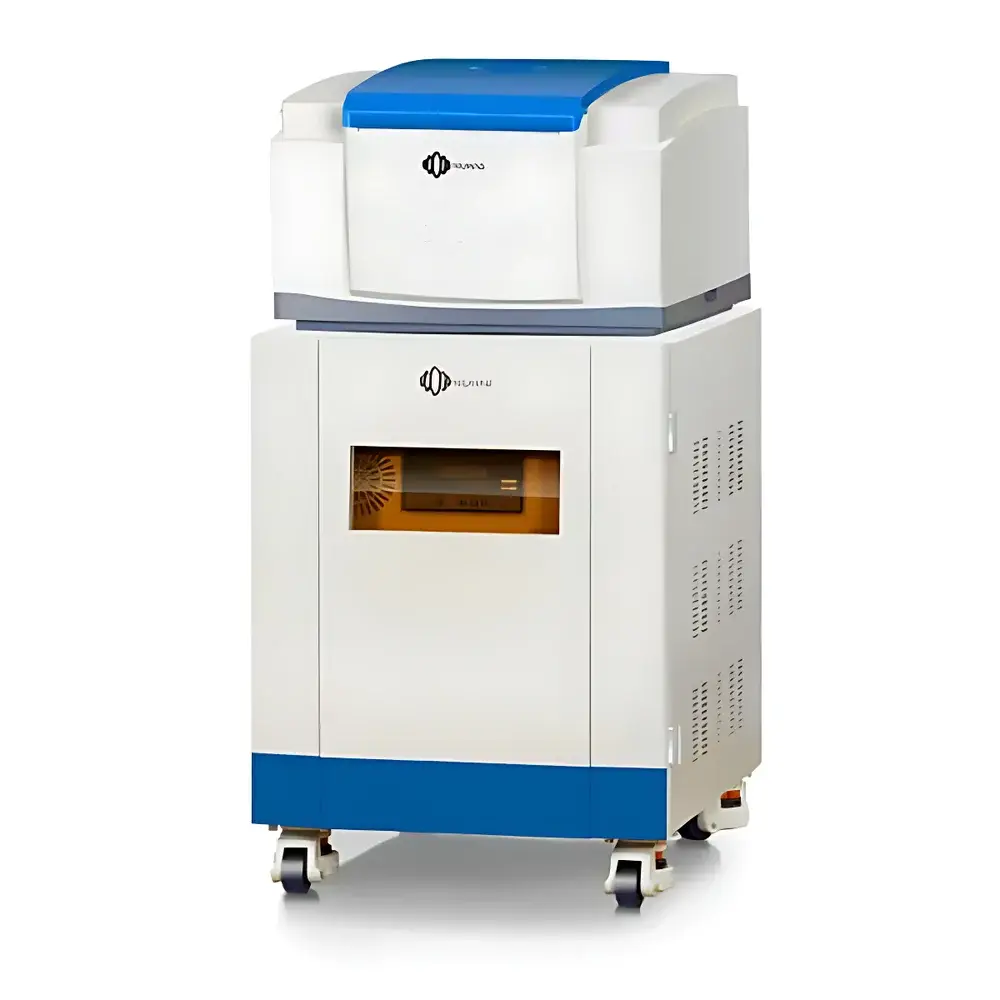
| Brand | NIUMAG |
|---|---|
| Origin | Jiangsu, China |
| Manufacturer Type | Authorized Distributor |
| Product Origin | Domestic (China) |
| Model | PQ Series |
| Pricing | Available Upon Request |
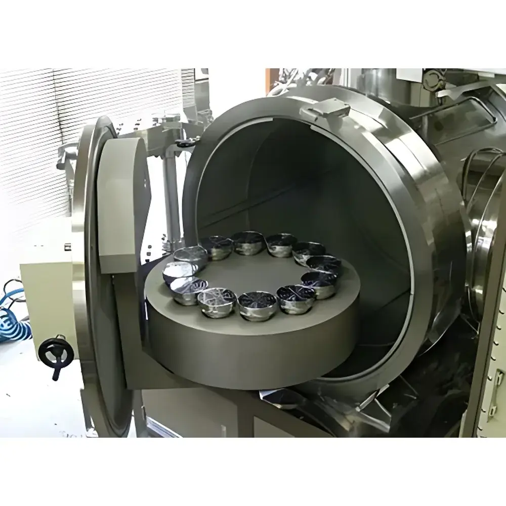
| Brand | NS (Japan) |
|---|---|
| Origin | Japan |
| Model | 20-M/NS-12 |
| Etching Principle | Kaufman-Type Ion Beam Etching (Physical Sputtering) |
| Substrate Capacity | 12 × 4-inch wafers OR 3 × 18-inch substrates |
| Ion Source | 20 cm Diameter Kaufman Ion Source (KRI Original, WELL-5100 Power Supply Standard) |
| Sample Stage | Direct Liquid-Cooled Electrode with Planetary Rotation (Rotation + Revolution) |
| Beam Tilt Adjustment | Motorized ±15° Continuous Adjustment |
| Cooling Method | Integrated Direct Chilled Stage (Temperature Control Enabled During Etch) |
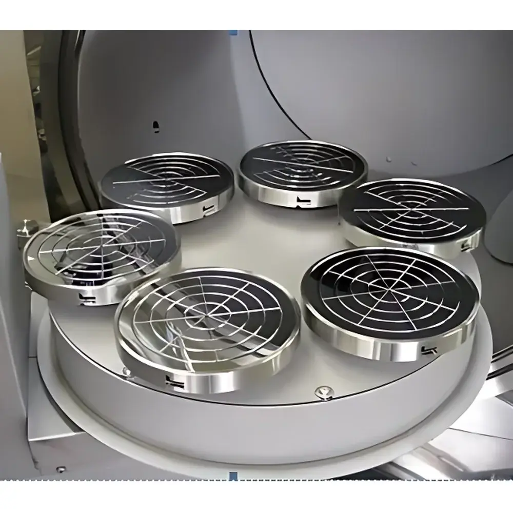
| Brand | NS (Japan) |
|---|---|
| Origin | Japan |
| Model | 20-M/NS-8 |
| Minimum Feature Size | 1 µm |
| Ion Beam Diameter | 1 µm |
| Acceleration Voltage Range | 1–5 kV (typical for Kaufman-type sources) |
| Substrate Capacity | 8 × Ø76 mm or 6 × Ø100 mm |
| Ion Source | 20 cm Kaufman-type Broad-Beam Ion Source (KRI, USA) |
| Cooling | Direct substrate cooling via integrated chiller interface |
| Motion Control | Planetary rotation (rotation + revolution) for uniform etch rate distribution |
| Power Supply | WELL-5000 (compatible with domestic replacements) |
| Compliance | CE-marked architecture |
| Brand | NS |
|---|---|
| Origin | Japan |
| Model | 4 IBE |
| Sample Holder | 4" φ, single wafer |
| Ion Incidence Angle | 0° to ±90° |
| Ion Source | KDC-40 Kaufman-type (KRI, USA) |
| Base Pressure | ≤1×10⁻⁴ Pa |
| Turbomolecular Pump | Pfeiffer, 350 L/s |
| Etch Uniformity | ≤±5% |
| Cooling | Direct substrate cooling |
| Motion Control | Planetary rotation (rotation + revolution) |
| Gas Compatibility | Ar, O₂, N₂, CF₄, Xe, and mixed process gases |
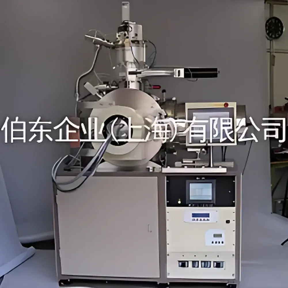
| Brand | NS (Nippon Seiko) |
|---|---|
| Origin | Japan |
| Model | NS-8 |
| Minimum Feature Size | ≤1 µm |
| Ion Beam Diameter | ≤1 mm |
| Acceleration Voltage Range | 0.5–2 kV |
| Substrate Capacity | 3″ wafers × 8 pcs or 4″ wafers × 6 pcs |
| Stage Cooling | Direct-contact liquid-cooled chuck (20 cm diameter) |
| Ion Source | Kaufman-type broad-beam ion source (OEM from Kimball Physics / original Kaufman design heritage) |
| Beam Tilt Adjustment | ±15° continuous RF-driven angular control |
| Substrate Motion | Dual-axis rotation (planetary motion: rotation + revolution) |
| Power Supply Compatibility | 200–240 VAC, 50/60 Hz (field-replaceable with domestic-standard AC input modules) |
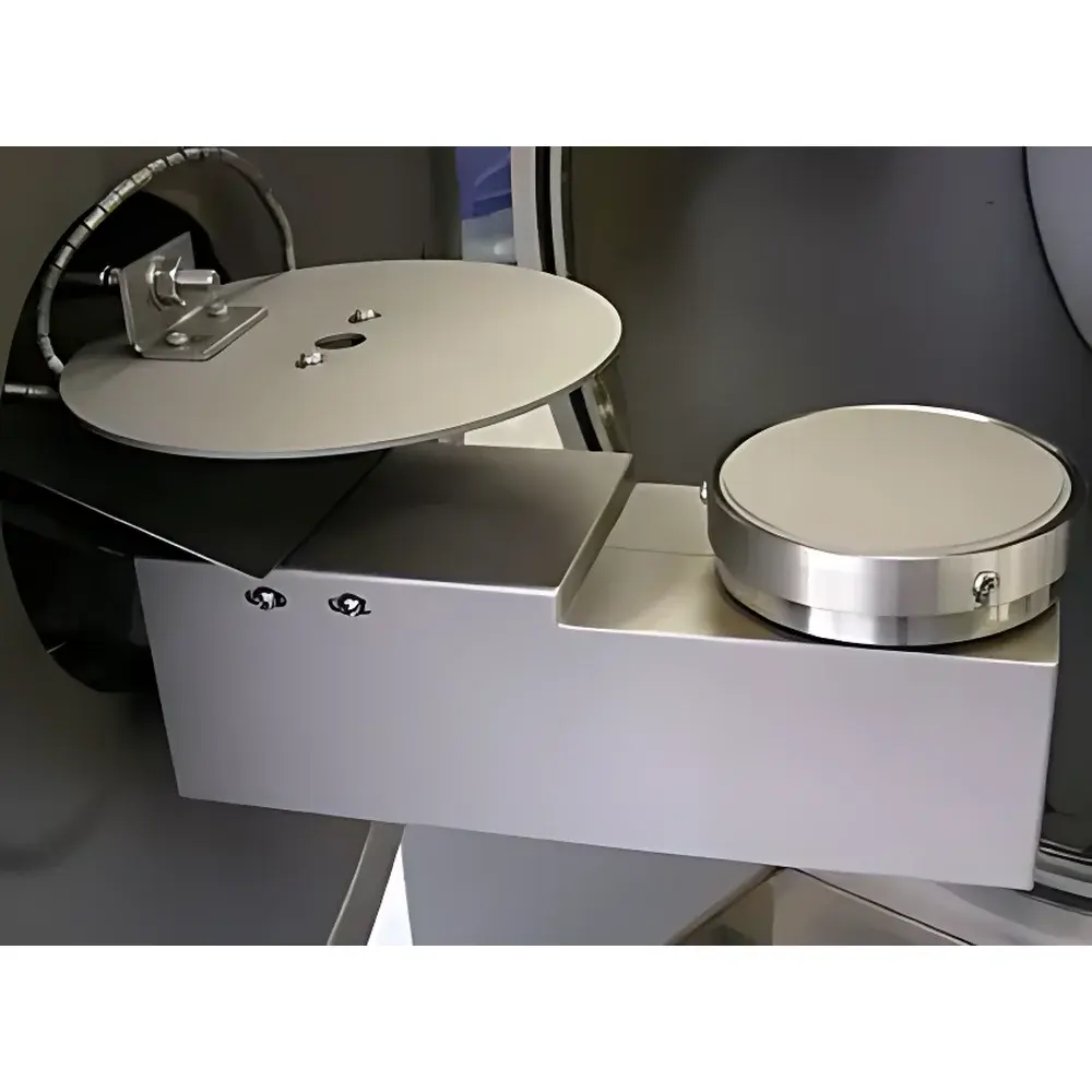
| Origin | Japan |
|---|---|
| Manufacturer Type | Authorized Distributor |
| Origin Category | Imported |
| Model | 10-M/NS-5 |
| Price Range | USD 135,000 – 205,000 |
| Substrate Diameter | 6-inch (150 mm) |
| Cooling | Direct substrate cooling with independent ion source cooling |
| Ion Source | 10 cm Kaufman-type ion source (KRI OEM) |
| Power Supply | WELL-2000 (compatible with domestic AC input upon request) |
| Beam Tilt | Adjustable RF-driven angular control (0°–90°) |
| Motion Control | Planetary rotation (substrate revolution + spin) |
| Process Environment | High-vacuum compatible (≤1×10⁻⁵ Pa base pressure, typical operating range 1×10⁻⁴–5×10⁻³ Pa) |
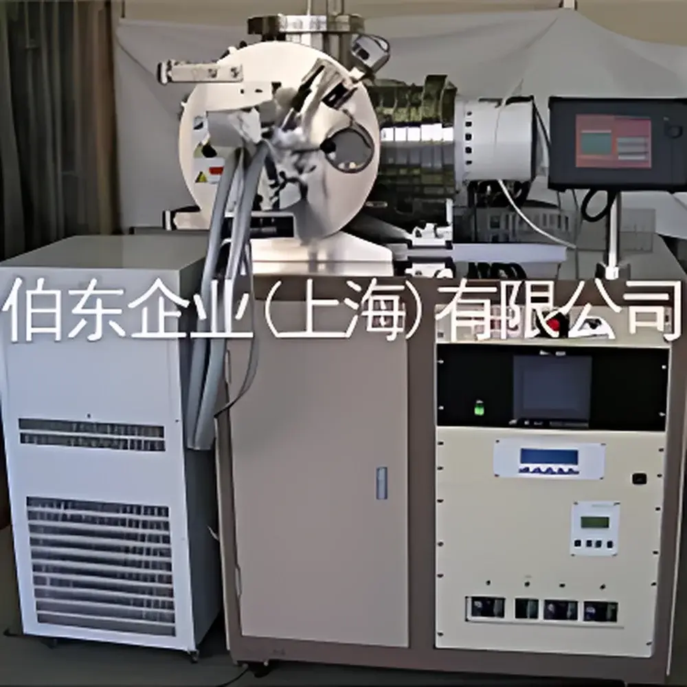
| Brand | NS |
|---|---|
| Origin | Japan |
| Model | NS-5 |
| Ion Source Type | Kaufman-type |
| Beam Diameter | 10 cm |
| Sample Stage Cooling | Direct-contact cryogenic cooling |
| Stage Motion | Combined rotation and revolution |
| Beam Tilt Adjustment | Fully variable (0–90°) |
| Application Scope | R&D and low-volume production |
| Substrate Compatibility | Up to 6-inch diameter wafers |
| Power Supply Compatibility | Interchangeable with domestic 220 V / 50 Hz AC input |
| Compliance | Designed for ISO Class 5 cleanroom integration |
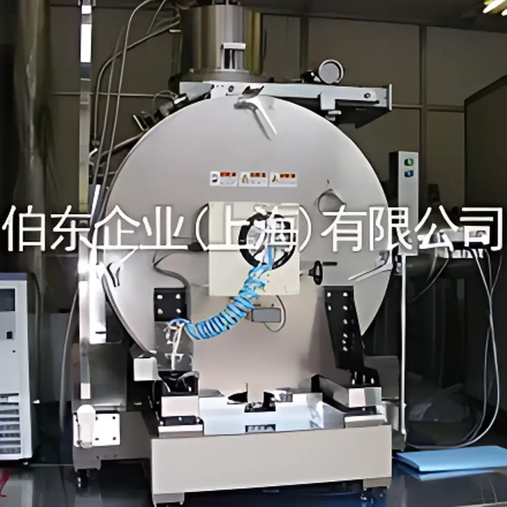
| Brand | NS |
|---|---|
| Origin | Japan |
| Model | NS-12 |
| Etching Principle | Broad-Beam Ion Beam Etching (IBE) |
| Substrate Capacity | 12 × Ø4″ wafers or 3 × Ø18″ wafers |
| Cooling | Direct substrate cooling via chilled chuck |
| Ion Source | 20 cm Kaufman-type ion source (original equipment from Kimball Physics / formerly Kaufman & Robinson) |
| Beam Steering | Adjustable incidence angle (0°–75°) |
| Rotation Mechanism | Independent planetary rotation (substrate rotation + revolution) |
| Residue-Free Processing | Yes |
| Power Supply Compatibility | Dual-voltage input (100 V / 200 V AC, 50/60 Hz) |
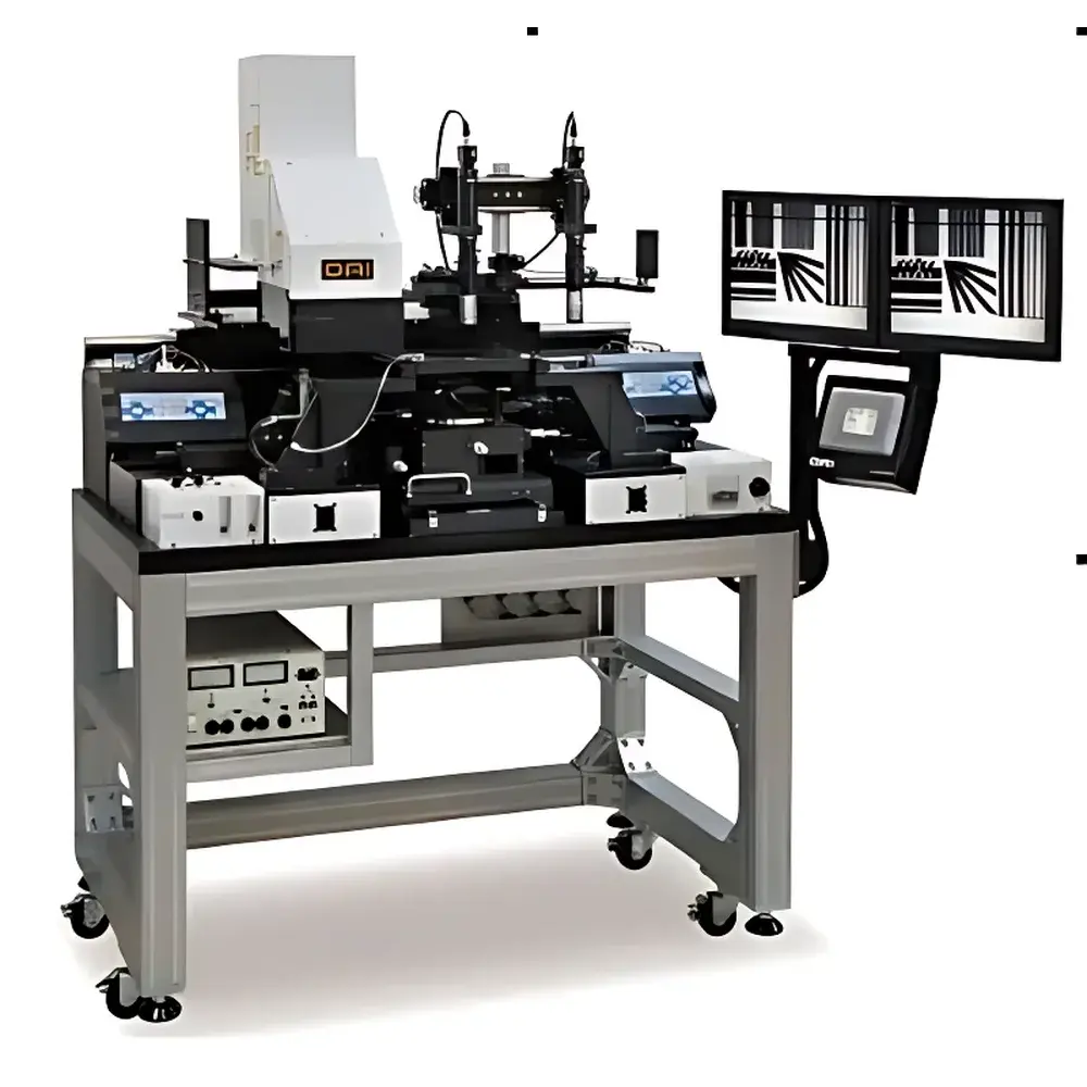
| Brand | OAI |
|---|---|
| Origin | USA |
| Model | MODEL 800MBA |
| Exposure Modes | Proximity, Soft Contact, Hard Contact, Vacuum Contact |
| Maximum Mask Size | 9" × 9" (228.6 mm × 228.6 mm) |
| Maximum Wafer Size | 200 mm (8-inch) |
| Light Source Type | High-Uniformity Broadband UV Lamp System |
| Alignment Accuracy | ≤ ±0.5 µm (typical, with optional auto-alignment upgrade) |
| Baseplate Thermal Stability | < ±0.1 °C over 4 hours |
| Compliance | ASTM F39–22 (Photolithography Equipment), ISO 14644–1 Class 5 Cleanroom Compatible |
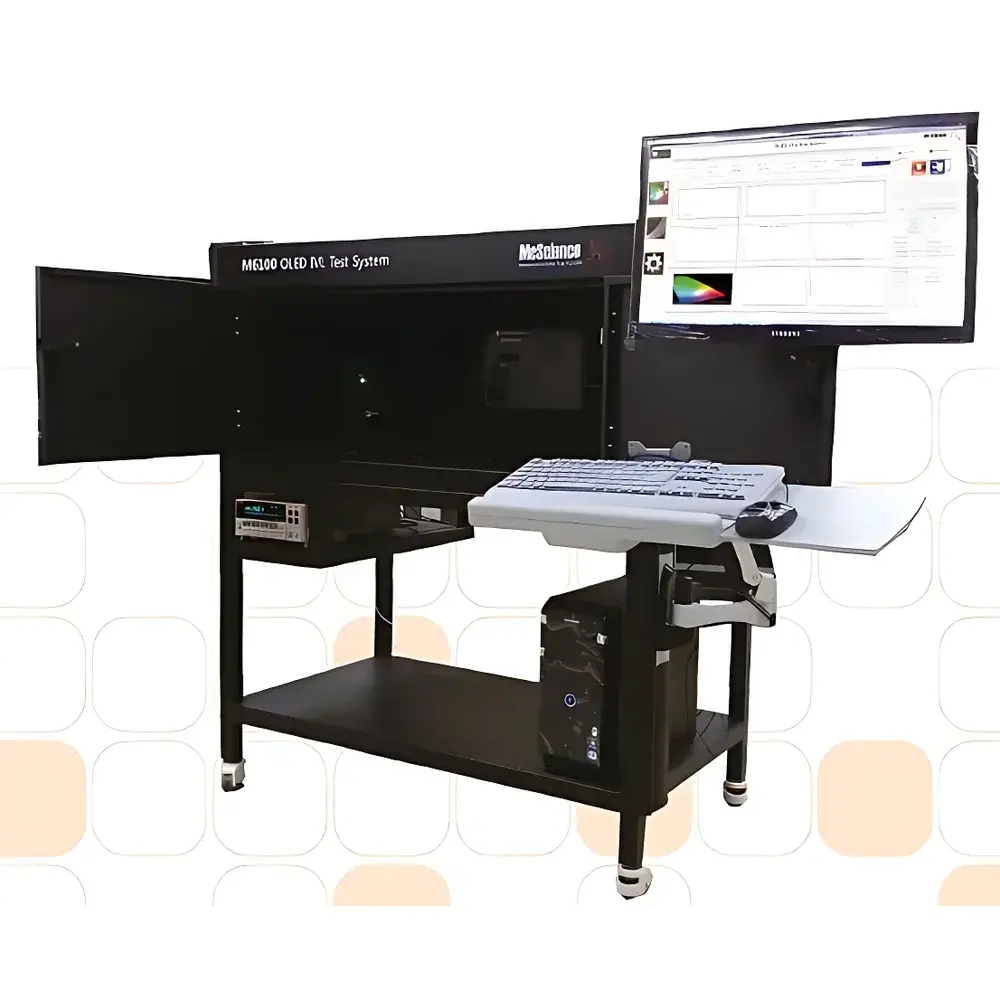
| Brand | McScience |
|---|---|
| Origin | South Korea |
| Model | M6100 |
| Instrument Type | Integrated Electroluminescence Characterization System for Organic and Emerging Light-Emitting Devices |
| Compliance | Designed for GLP-compliant lab environments |
| Electrical Source | Precision Source Measure Unit (SMU) |
| Optical Detection | Compatible with calibrated spectroradiometers and tristimulus colorimeters |
| Operating Environment | Light-tight enclosure with EMI-shielded chamber |
| Drive Modes | DC, pulsed, and programmable waveform injection |
| Sample Form Factor | Discrete devices, rigid/flexible substrates, micro-LED arrays, and active-matrix OLED panels |
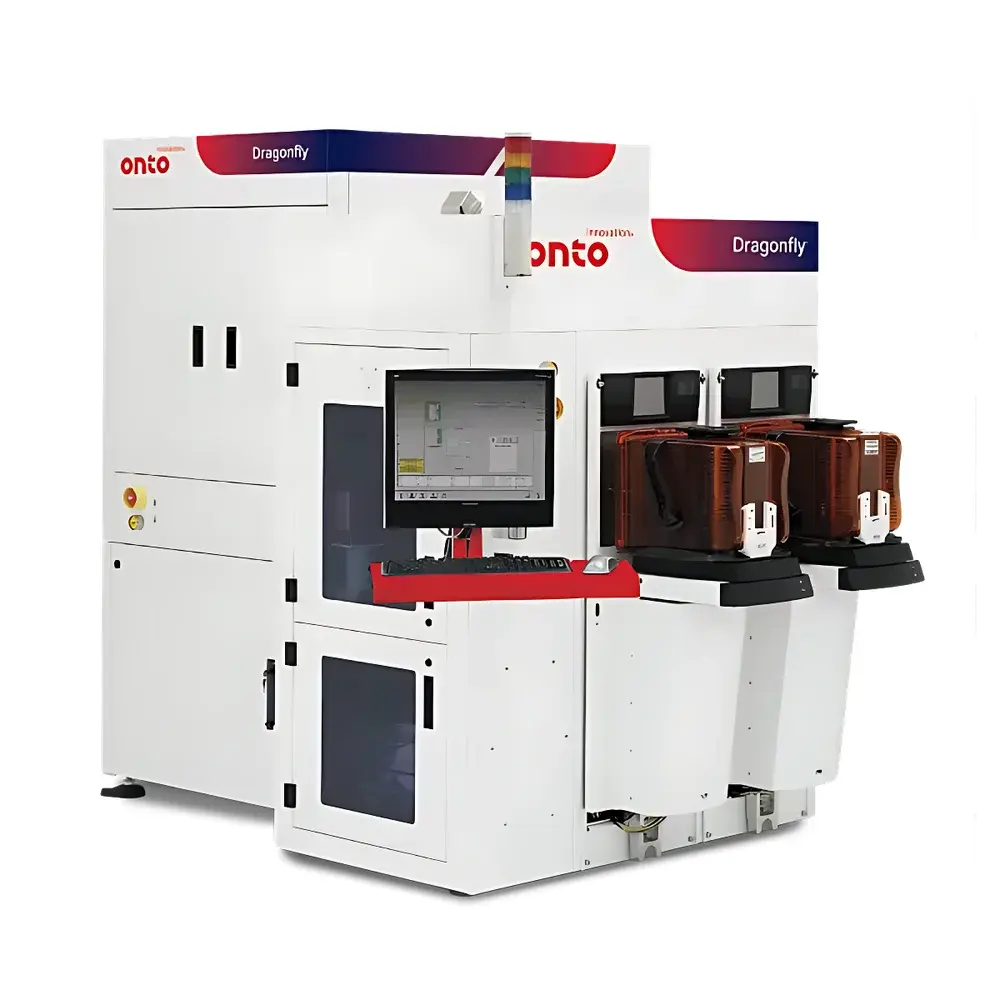
| Brand | Onto Innovation |
|---|---|
| Model | Dragonfly® G3 |
| Origin | Malaysia |
| Equipment Type | Inline AOI for Front-End & Advanced Packaging |
| Minimum Detectable Line Width/Spacing | 0.7 µm |
| Wafer Size Support | 100 mm – 330 mm |
| Maximum Substrate Area | >6400 mm² |
| 翘曲晶圆 & Taiko Handling | Supported |
| Imaging Modes | Brightfield, Darkfield, Oblique Illumination, IR Transmission |
| 3D Metrology | Truebump® (Multi-Modal 3D Profilometry) |
| Residue Detection | Clearfind® |
| Software Platform | nLINE™ with Real-Time Analysis, Offline Review, and Exploratory Bump-Level Data Analytics |
| Compliance Framework | Supports ASTM F2598 (Wafer Defect Classification), ISO 14644-1 (Cleanroom Integration), and GLP/GMP-aligned Audit Trail Logging |
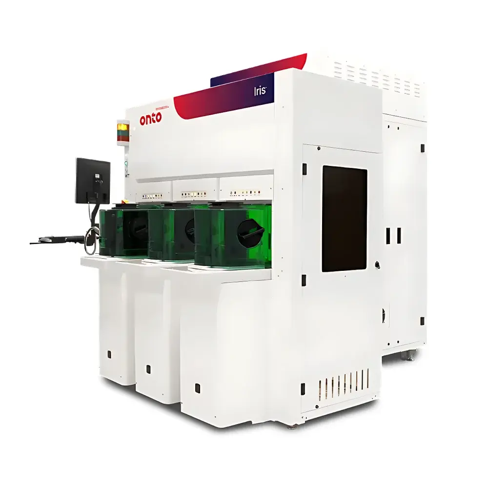
| Brand | AiYao Instruments |
|---|---|
| Origin | Malaysia |
| Manufacturer Type | Authorized Distributor |
| Origin Category | Imported |
| Model | IRIS S |
| Pricing | Available Upon Request |
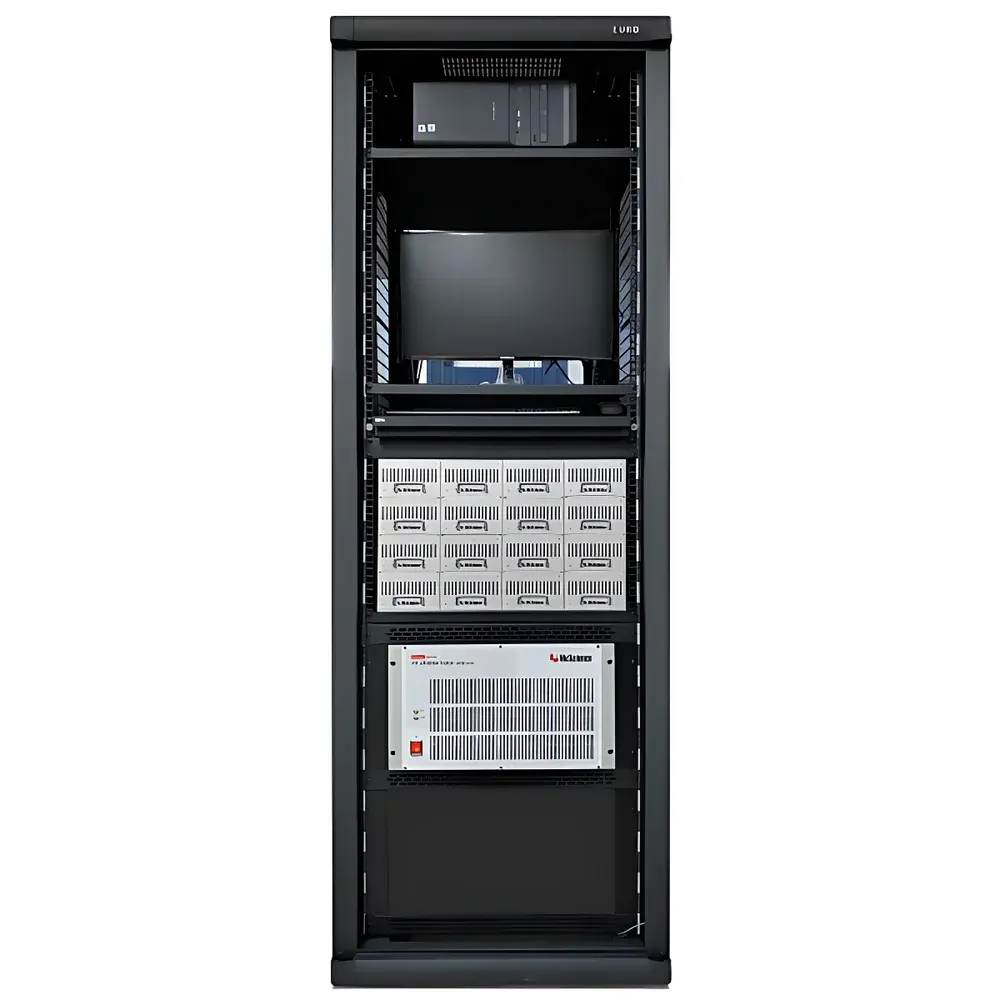
| Brand | McScience |
|---|---|
| Origin | South Korea |
| Model | OPD-LT |
| Channel Configuration | Multi-channel (configurable) |
| Spectral Range Options | UV to IR (200–1700 nm, selectable modules) |
| Compliance | ISO/IEC 17025-compatible test environment support |
| Software Control | PC-based with timestamped event logging and real-time degradation trend analysis |
| Operating Mode | Constant-bias or pulsed-bias stress testing under controlled ambient (N₂ glovebox or environmental chamber integration optional) |
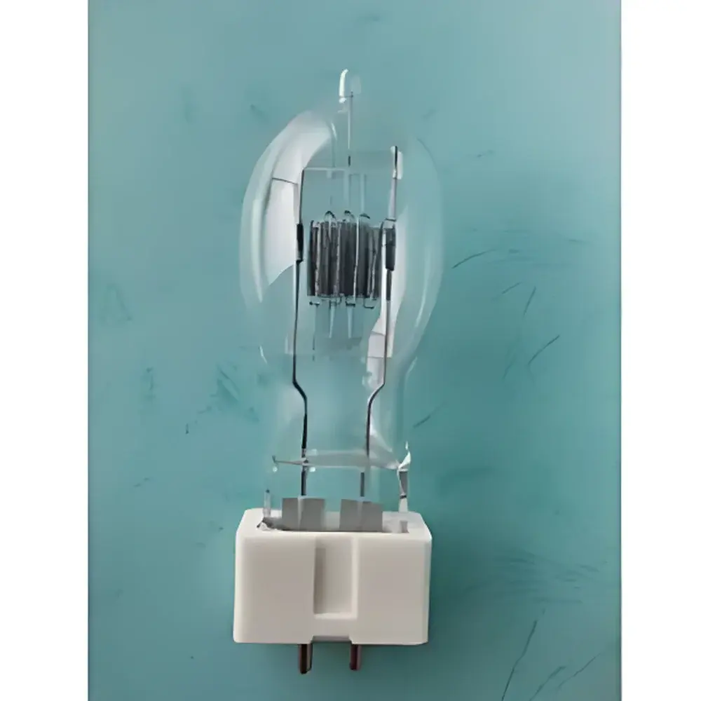
| Brand | CSC |
|---|---|
| Origin | Japan |
| Supplier Type | Authorized Distributor |
| Import Status | Imported |
| Model | Not Applicable |
| Pricing | Upon Request |