
Semiconductor Instruments
Filter
Showing 421–450 of 852 results
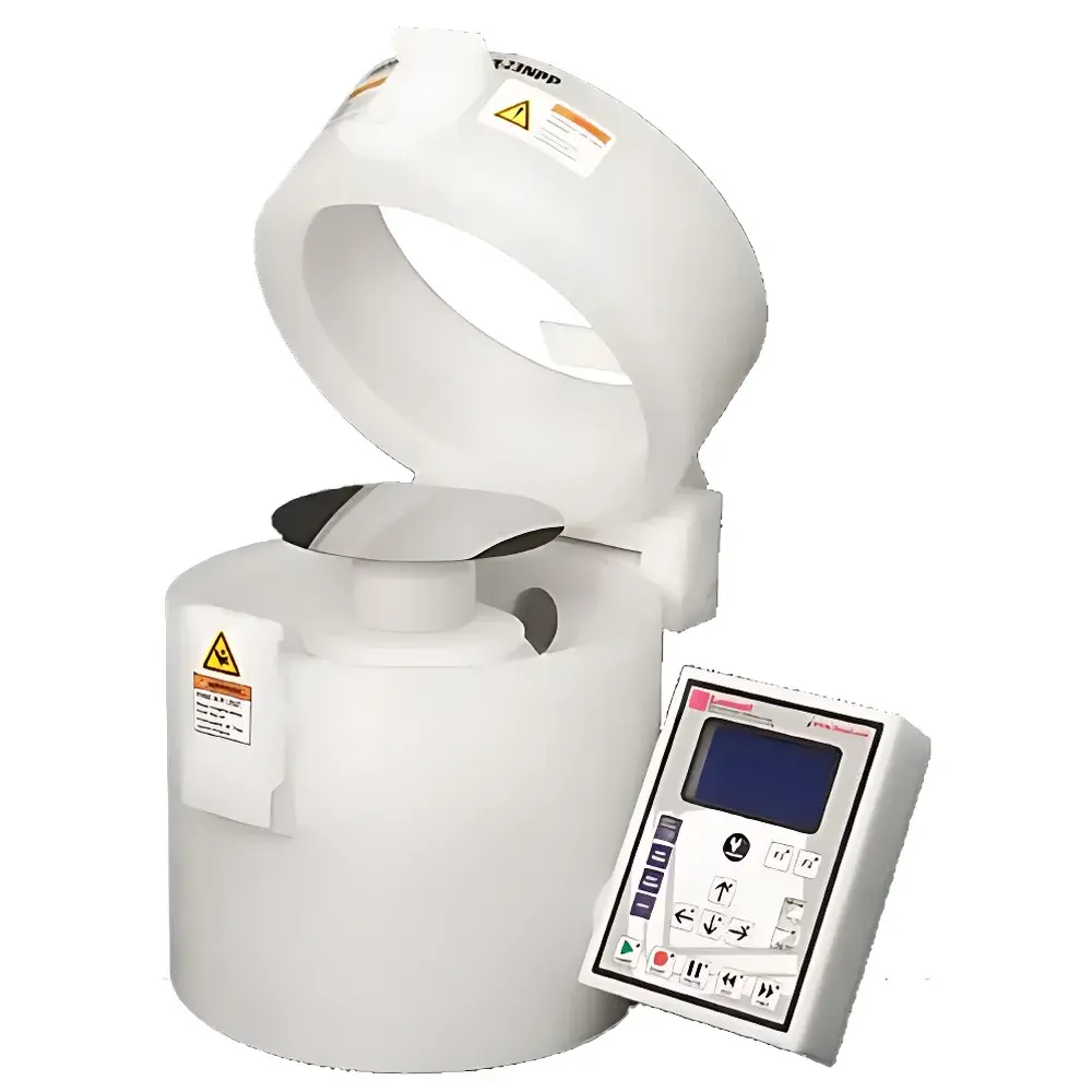
| Brand | Laurell |
|---|---|
| Origin | USA |
| Model | WS-650Mz-23N |
| Maximum Speed | 12,000 rpm |
| Acceleration | 0–12,000 rpm/sec |
| Speed Accuracy | ≤ ±1 rpm (NIST-traceable) |
| Speed Stability | < ±1% |
| Time Resolution | 0.1 sec (1–5999.9 sec/step) |
| Chuck Compatibility | Ø10–150 mm wafers or 125×125 mm square substrates |
| Chamber Diameter | 9.5 in (241 mm) |
| Controller | PLC-based with SPIN3000 software integration |
| Construction Material | NPP (Natural Polypropylene) |
| Programmability | 20 stored recipes, up to 51 steps per recipe |
| Vacuum System | Oil-free pump, 220–240 VAC, 50/60 Hz |
| Leveling | Included NIST-calibrated digital level |
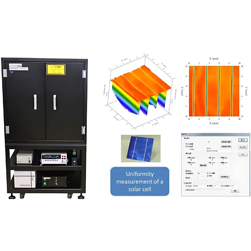
| Origin | Japan |
|---|---|
| Manufacturer Type | Authorized Distributor |
| Origin Category | Imported |
| Model | LBC-1 |
| Price Range | USD 110,000 – 138,000 |
| Laser Wavelength | 532 nm (Green) |
| Laser Power Output | 10 mW |
| Beam Stability | ±2% |
| Spot Size | Ø100 µm |
| Maximum Scan Area | 50 mm × 50 mm (X-Y Stage Travel: ±30 mm) |
| Photocurrent Measurement Range | 10 pA – 1 A (Keithley Model 2401) |
| Irradiation Configuration | Top-side or Bottom-side (Optional) |
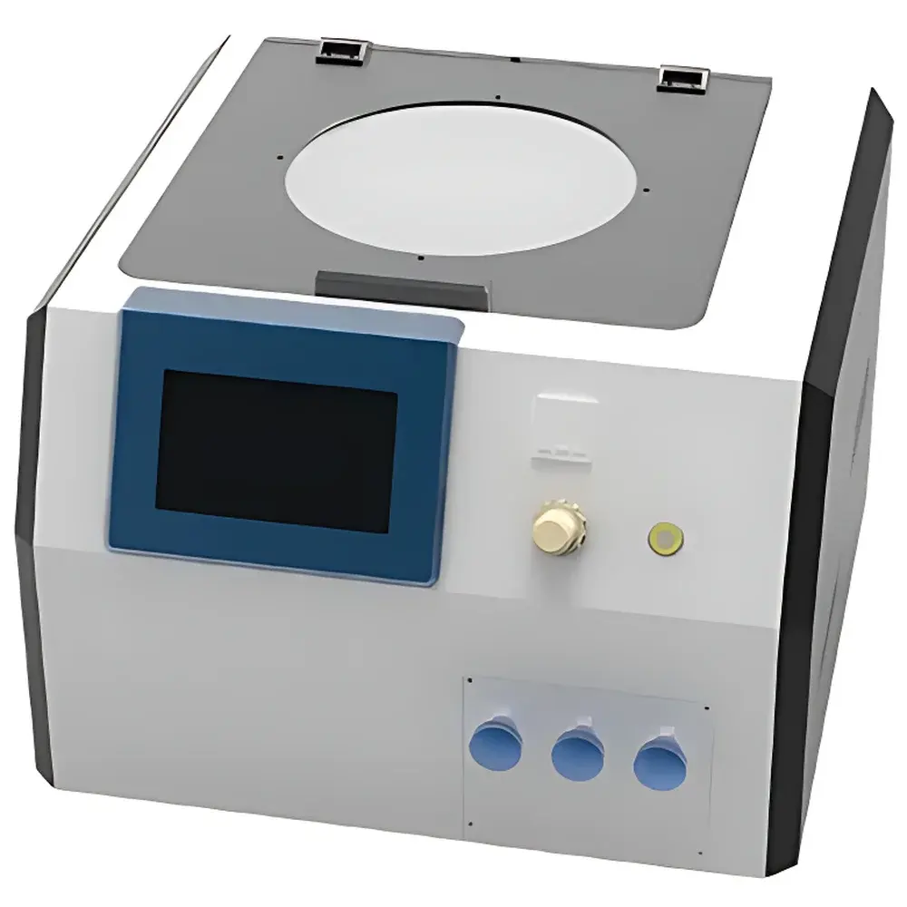
| Brand | LEBO Science |
|---|---|
| Origin | Imported |
| Manufacturer Type | Authorized Distributor |
| Model | Customized-2 |
| Wafer Compatibility | Fragments to 200 mm (customizable up to 300 mm with quad-nozzle configuration) |
| Development Modes | Single-step & Multi-step Programmable Process |
| Max. Spin Speed | 3000 rpm (no-load) |
| Speed Resolution | ±1 rpm |
| Acceleration Range | 10–10,000 rpm/sec (no-load) |
| Step Duration Range | 0–3000 sec |
| Time Resolution | 0.1 sec |
| Nozzle Control | Motorized XYZ-positioning with programmable trajectory |
| Fluid Delivery | 1 dedicated developer channel + 1 deionized water rinse channel + 1 N₂ purge channel |
| Compliance | Designed for Class 100–1000 cleanroom environments |
| Software | Onboard HMI with 100 user-editable process recipes |
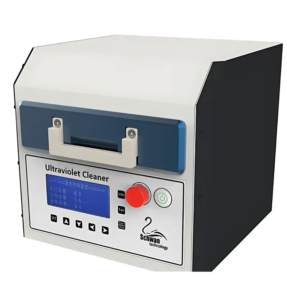
| Brand | LEBO Science |
|---|---|
| Origin | Jiangyin, Jiangsu, China |
| Model | UC100-SE |
| Rated Voltage | AC 220 V, 50 Hz |
| Lamp Power | 275–300 W |
| Lamp Lifetime | ≥8,000 h |
| Emission Wavelengths | 184/185 nm + 254 nm |
| Maximum Substrate Size | ≤8-inch (200 mm) |
| Dimensions (W×D×H) | 330 × 400–420 × 315 mm |
| Weight | 15–16 kg |
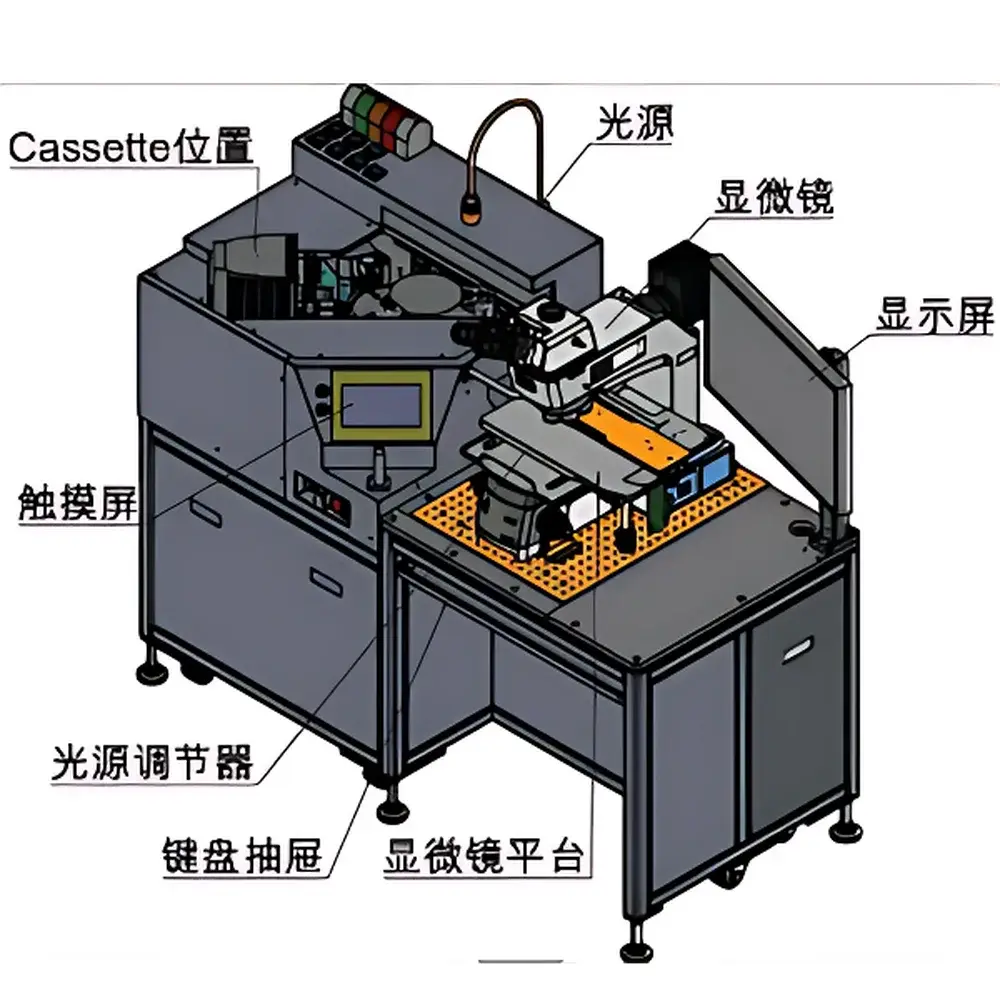
| Brand | LEI-TECH |
|---|---|
| Origin | Tianjin, China |
| Manufacturer Type | Original Equipment Manufacturer (OEM) |
| Product Category | Domestic |
| Model | LK-BY86 |
| Pricing | Upon Request |
| Instrument Type | Optical Patterned Defect Inspection System |
| Primary Applications | Front-end & back-end wafer process monitoring, outgoing wafer quality control, automated wafer handling |
| Compatible Wafer Diameters | 150 mm (6″), 200 mm (8″), 300 mm (12″) |
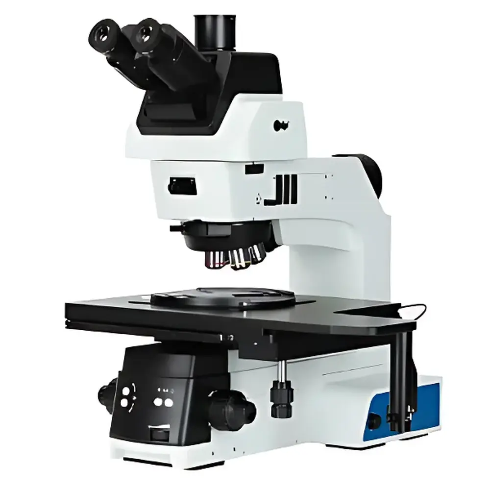
| Brand | LEI-TECH |
|---|---|
| Origin | Tianjin, China |
| Manufacturer Type | OEM Manufacturer |
| Product Category | Domestic |
| Model | LK-ZDJY80R |
| Instrument Class | Optical Patterned Defect Inspection System |
| Primary Applications | Wafer process monitoring, outgoing wafer quality control |
| Compatible Wafer Sizes | 4", 6", 8", 12" |
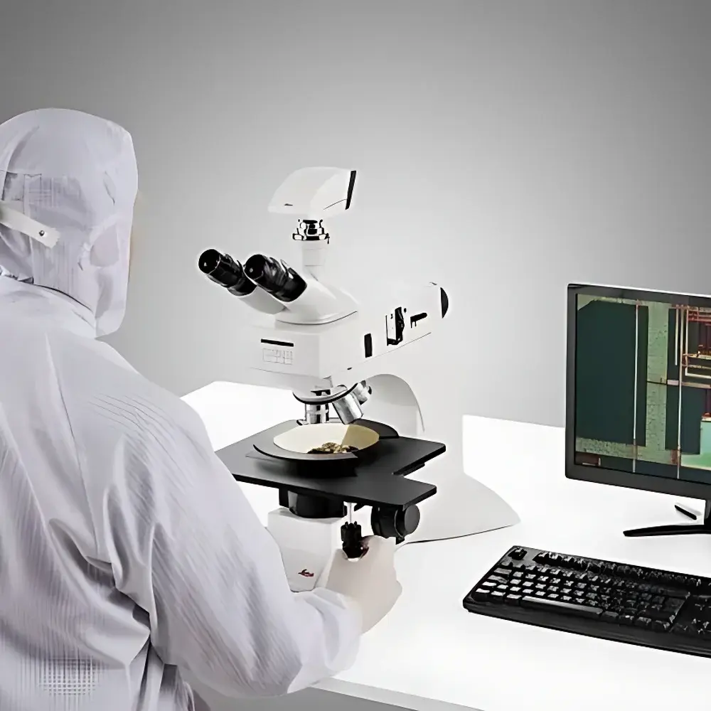
| Brand | Leica |
|---|---|
| Origin | Germany |
| Manufacturer Type | Authorized Distributor |
| Origin Category | Imported |
| Model | DM3 XL |
| Pricing | Upon Request |
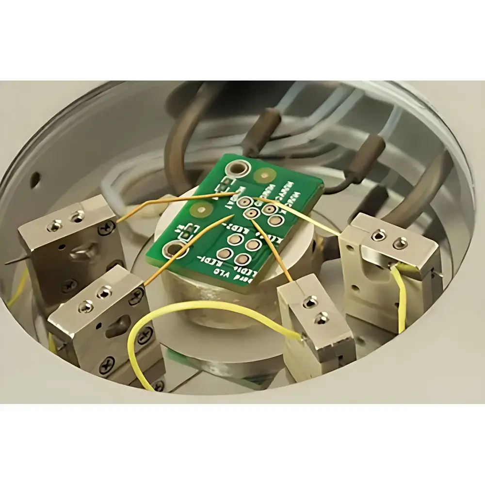
| Brand | Linkam |
|---|---|
| Origin | United Kingdom |
| Model | LTS420E-P |
| Temperature Range | Ambient to +420 °C (with optional cryogenic cooling to −196 °C) |
| Electrode Configuration | Integrated dual-electrode system |
| Temperature Control Accuracy | ±0.01 °C |
| Temperature Stability | <0.01 °C |
| Optical Aperture Diameter | 2.4 mm |
| Sample Translation Range (X–Y) | 15 × 15 mm |
| Active Sample Area | 53.5 × 43 mm |
| Compatible Substrates | Standard 76 × 26 mm microscope slides or φ16 mm coverslips |
| Heating Rate | 0.1–50 °C/min |
| Minimum Working Distance (Objective/Condenser) | 6.0 mm / 13.2 mm |
| Stage Dimensions | 160 × 80 × 24 mm |
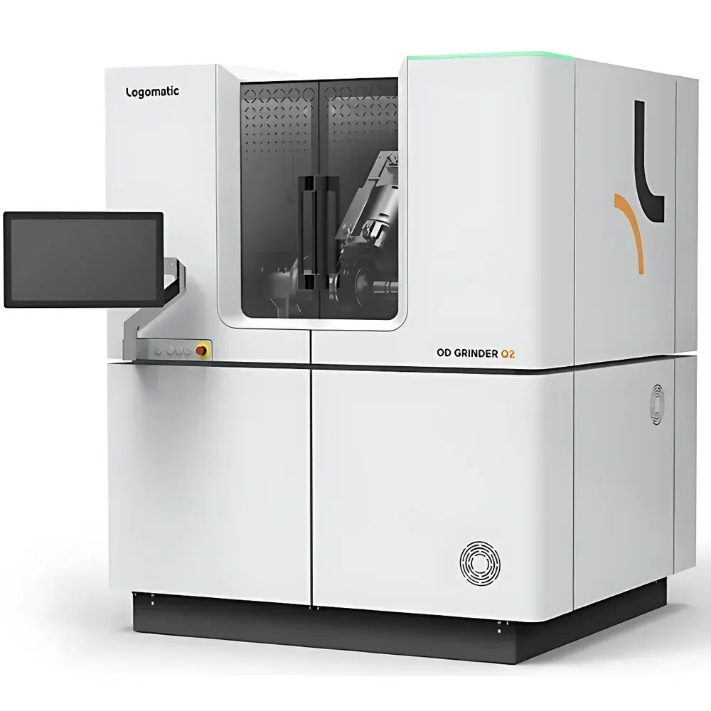
| Brand | Logomatic |
|---|---|
| Origin | Germany |
| Model | Q2/Q2+ |
| Applicable Wafer Sizes | 6" and 8" |
| Max Ingot Length | 60 mm |
| Chuck Center Height | 125 mm |
| Machine Dimensions (L×W×H) | 1.8 m × 1.8 m × 1.9 m |
| Weight | 4.5 ton |
| Power Consumption | 4 kW |
| Spindle Speed | 3500 rpm |
| Integrated X-ray Orientation System | Yes |
| Peel Grinding Technology | Yes |
| Automated Notch & Flat Machining | Yes |
| Optical Notch Profile Inspection | Yes |
| Real-time Acoustic Emission & Force Sensing | Yes |
| Digital Twin Process Simulation | Yes |
| Centrifugal Pure Water Supply System (shared across up to 8 units) | Yes |
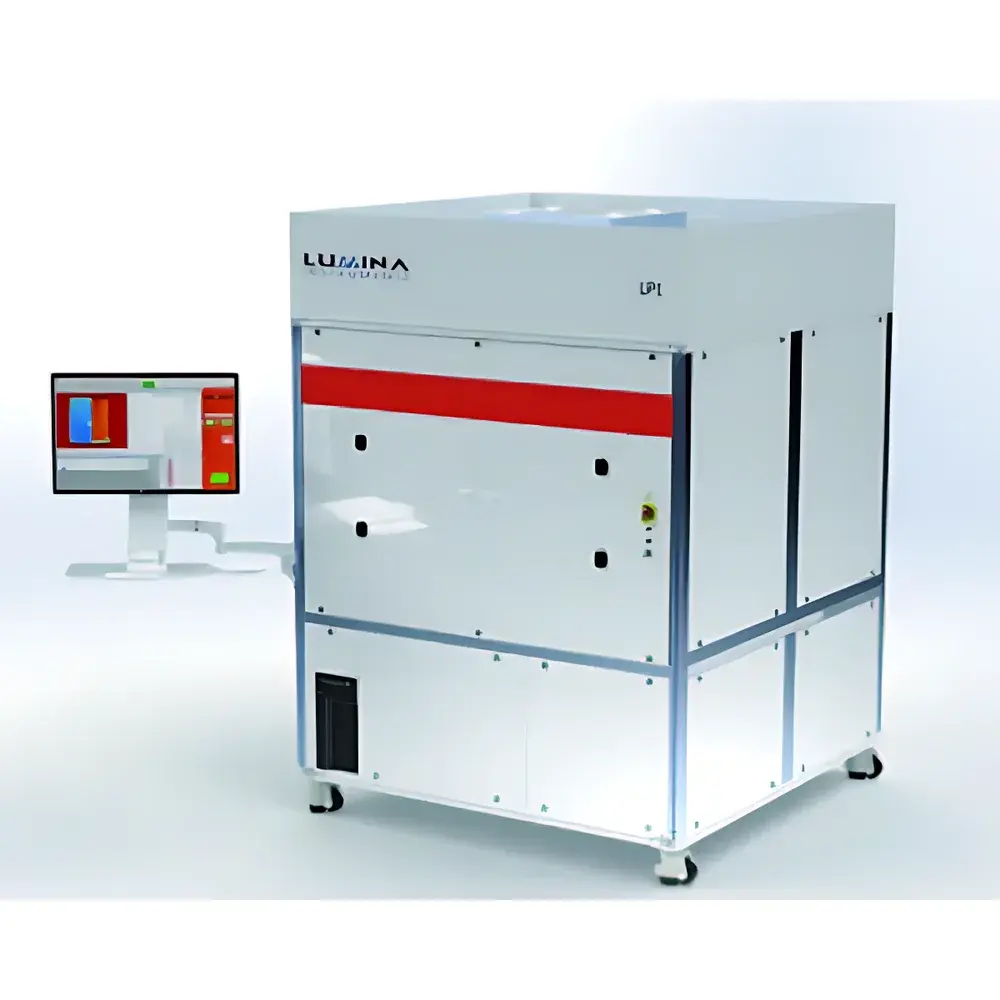
| Brand | Lumina |
|---|---|
| Origin | USA |
| Manufacturer Type | Authorized Distributor |
| Origin Category | Imported |
| Model | AT Series (AT1, AT1-Auto, AT2, AT2-EFEM) |
| Pricing | Available Upon Request |
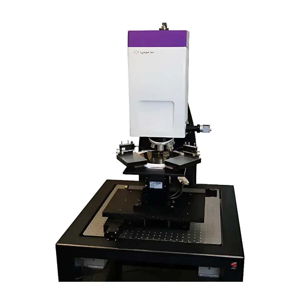
| Brand | LynceeTec |
|---|---|
| Origin | Switzerland |
| Model | DHM R1000 MEMS |
| Measurement Principle | Digital Holographic Interferometry (DHI) |
| Operating Mode | Non-contact, Full-field, Single-shot 4D Imaging (3D topography + time) |
| Vertical Resolution | ≤5 pm |
| In-plane Displacement Resolution | ≤1 nm (sub-pixel algorithm) |
| Maximum Excitation Frequency | 25 MHz |
| Frame Rate | Up to 1.25 MHz (with burst mode) |
| Software | MEMSAnalysis Tool v5.x |
| Compliance | ASTM E2558, ISO/IEC 17025-compatible workflows, FDA 21 CFR Part 11 audit trail support (optional), GLP/GMP-ready metadata logging |
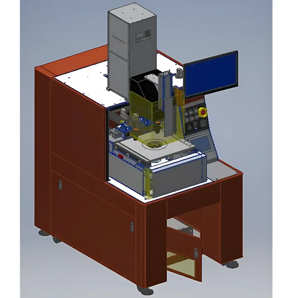
| Brand | M&R |
|---|---|
| Origin | Taiwan |
| Model | AA-8N-LED |
| Light Source | UV LED |
| Maximum Substrate Size | ≤4-inch wafers (including irregular shapes) |
| Overlay Alignment Accuracy | ±1 µm |
| Optical Resolution | ≤1 µm |
| Configuration | Standalone benchtop system for contact-mode lithography and manual/semi-automated bond alignment |
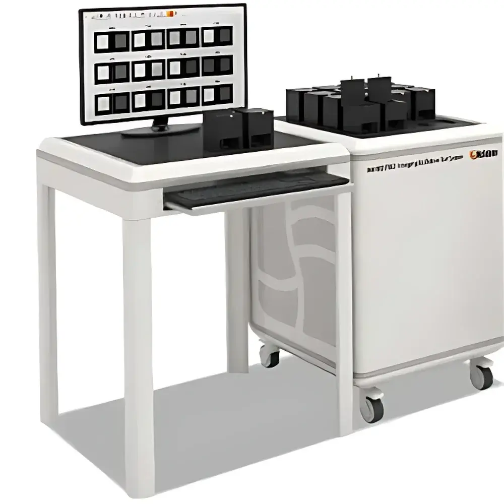
| Brand | McScience |
|---|---|
| Origin | South Korea |
| Model | M6000 PIXX |
| Device Type | Imaging-Based Electroluminescence Degradation Analyzer |
| Application Domain | Perovskite LED, OLED, QLED, Flexible Optoelectronic Devices, Inkjet-Printed Emissive Layer Development |
| Compliance Context | Designed for GLP-compliant lifetime testing workflows |
| Software Architecture | Windows-based acquisition and spatiotemporal EL intensity mapping platform |
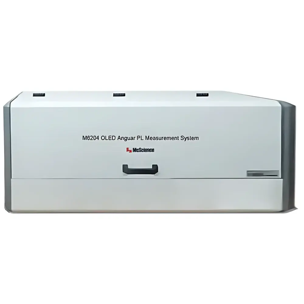
| Brand | McScience |
|---|---|
| Origin | South Korea |
| Model | M6204 |
| Type | Import Instrument |
| Distribution Channel | Authorized Distributor |
| Pricing | Upon Request |
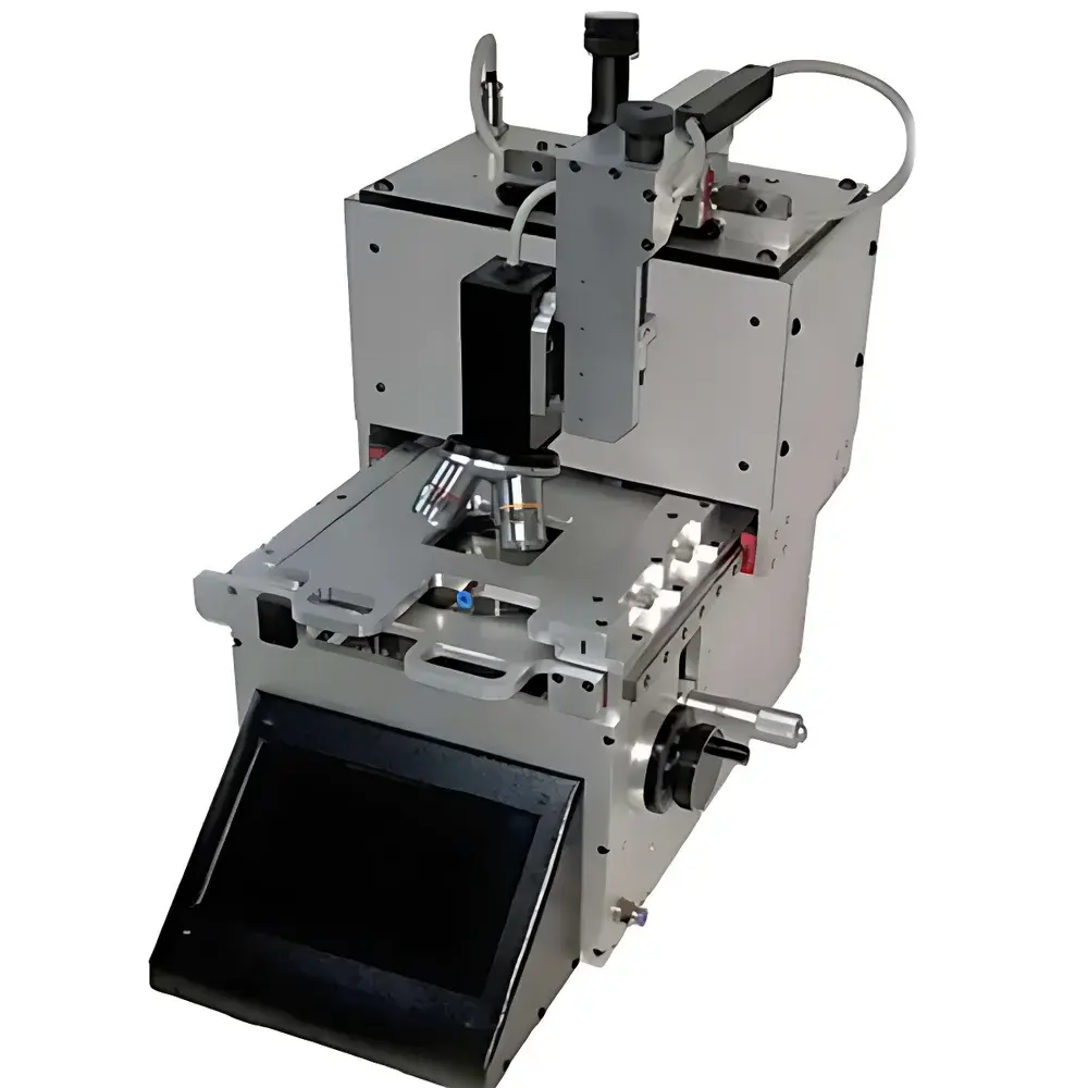
| Brand | Makeway |
|---|---|
| Origin | USA |
| Model | MKW-280 |
| Mask Size | 5 in |
| Wafer/Substrate Size | 5 in |
| Alignment Accuracy | 1 µm (Vacuum Contact), 1.5 µm (Hard Contact), 3 µm (Soft Contact), 5 µm (Proximity Mode) |
| UV Source | 350 W, 365 nm, uniformity ±3%, irradiance 30 mW/cm² |
| Exposure Time Range | 0.1–999 s |
| Chuck Motion | Manual X/Y/Z/θ with wedge compensation leveling |
| Microscopy | Dual CCD-based system, 80×–400× standard, up to 1000× with optional lenses, working distance 50–150 mm |
| Display | 20" LCD monitor |
| Contact Modes | Vacuum contact (adjustable force), hard contact, soft contact, proximity (gap adjustable) |
| Power Supply | 220 V, single-phase, 15 A |
| Optional | Deep UV source, IR alignment mode, custom substrate chucks |
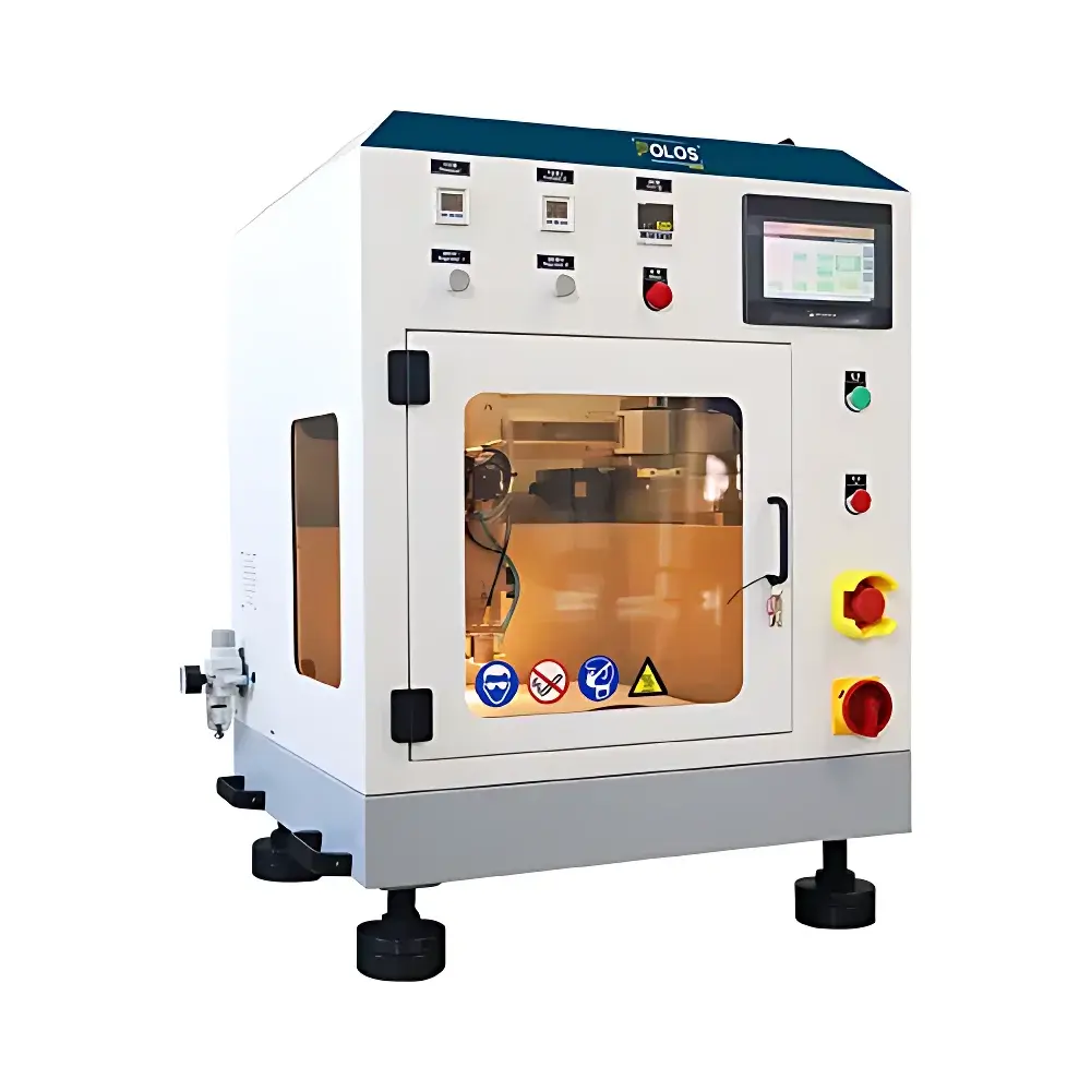
| Brand | Makeway |
|---|---|
| Origin | Shanghai, China |
| Manufacturer Type | Authorized Distributor |
| Region of Origin | Domestic (China) |
| Model | MKW-320 |
| Price Range | USD 21,000 – 55,000 |
| Brand | Makeway |
|---|---|
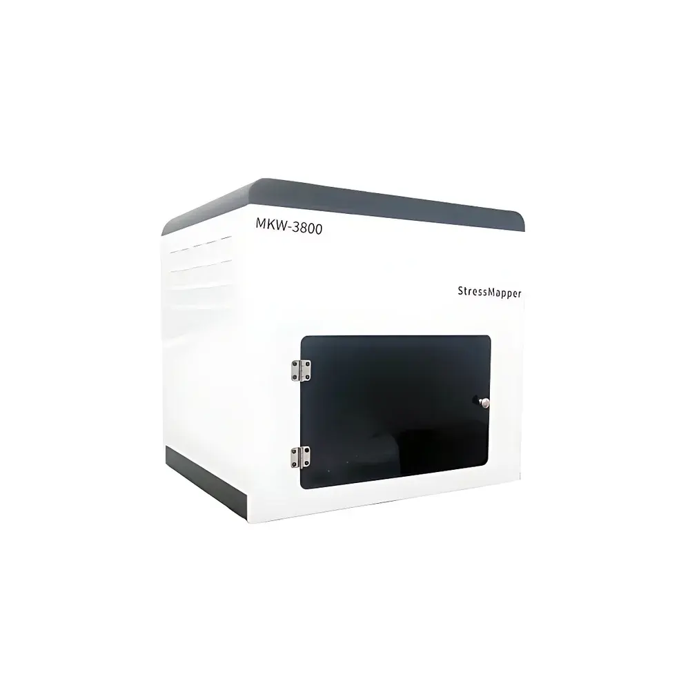
| Model | MKW-3800 |
| Origin | Shanghai, China |
| Measurement Principle | Non-contact structured light reflectometry |
| Sample Diameter | 2–8 inch wafers |
| Sampling Interval | down to 0.1 mm (full-field uniform sampling) |
| Measurement Time | <30 s (for 6-inch wafer, full aperture) |
| Warpage Range | 0.5–5000 µm |
| Warpage Repeatability | ±0.2 µm or ±1% |
| Warpage Accuracy | ±0.5 µm or ±1.5% |
| Stress Range | 1–10,000 MPa |
| Curvature Radius Range | 0.5–10,000 m |
| Curvature Repeatability | <1% (1σ @ 25 m radius) |
| Stress Repeatability | ±1.5 MPa or ±1% |
| Compatible Substrates | Si, GaAs, LiTaO₃, glass, sapphire, InP, SiC, GaN, bonded wafers, patterned wafers, square optical substrates |
| Compatible Films | Si, SiO₂, SiNₓ, Al₂O₃, TiO₂, photoresist, metal films, adhesives, nano-polymeric films, hybrid organic/inorganic films |
| Software | Stress Mapper (real-time acquisition, Stoney equation-based stress calculation, polynomial fitting, spatial filtering, ROI analysis, time-resolved & temperature-dependent stress profiling) |
| Brand | Makeway |
|---|---|
| Model | MKW-2800 |
| Measurement Principle | 3ω Method |
| Temperature Control Range | Ambient to 200 °C (typical for thin-film thermal characterization) |
| Electrical Excitation Frequency | 1–10 Hz (optimized for 3ω harmonic detection) |
| Thermal Conductivity Range | 0.1–500 W/(m·K) |
| Resolution | <±2% (relative, under controlled lab conditions) |
| Compliance | ASTM E1461, ISO 22007-4, USP <1031> (thermal property validation) |
| Software Interface | Windows-based with real-time data acquisition, harmonic phase analysis, and temperature-swept conductivity mapping |
| Brand | SUSS MicroTec |
|---|---|
| Origin | Germany |
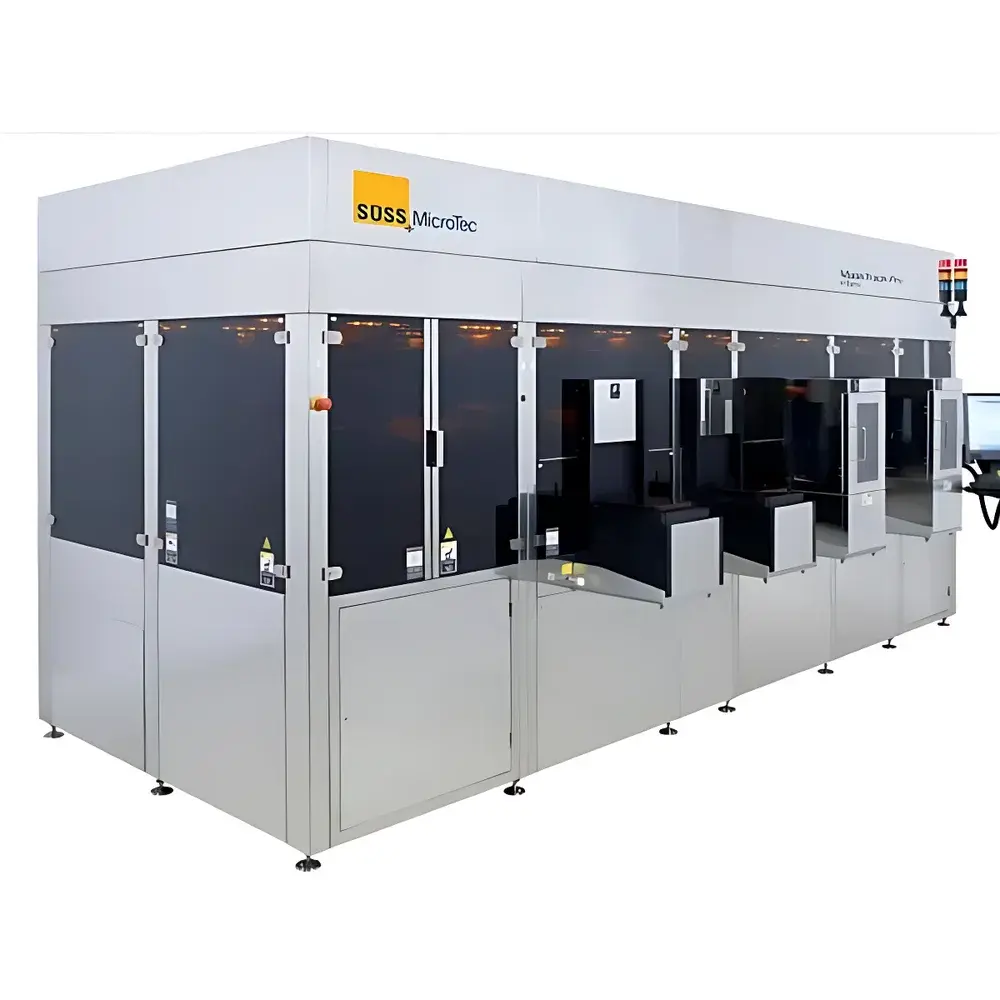
| Model | MaskTrack Pro |
| Application Scope | Automated cleaning, bake, and develop for photomasks & reticles |
| Compatibility | 90 nm to sub-1x nm half-pitch nodes |
| Process Capabilities | Front-side & backside cleaning, sulfur-free chemistry option, integrated particle detection readiness |
| Architecture | Cluster-compatible platform (with InSync, backside particle inspection, EUV mask storage) |
| Regulatory Context | Designed for ISO Class 1–5 cleanroom integration, supports GLP/GMP-aligned process documentation |
| Brand | Truth Instruments Company Limited |
|---|---|
| Origin | Anhui, China |
| Manufacturer Type | Authorized Distributor |
| Origin Category | Domestic (PRC) |
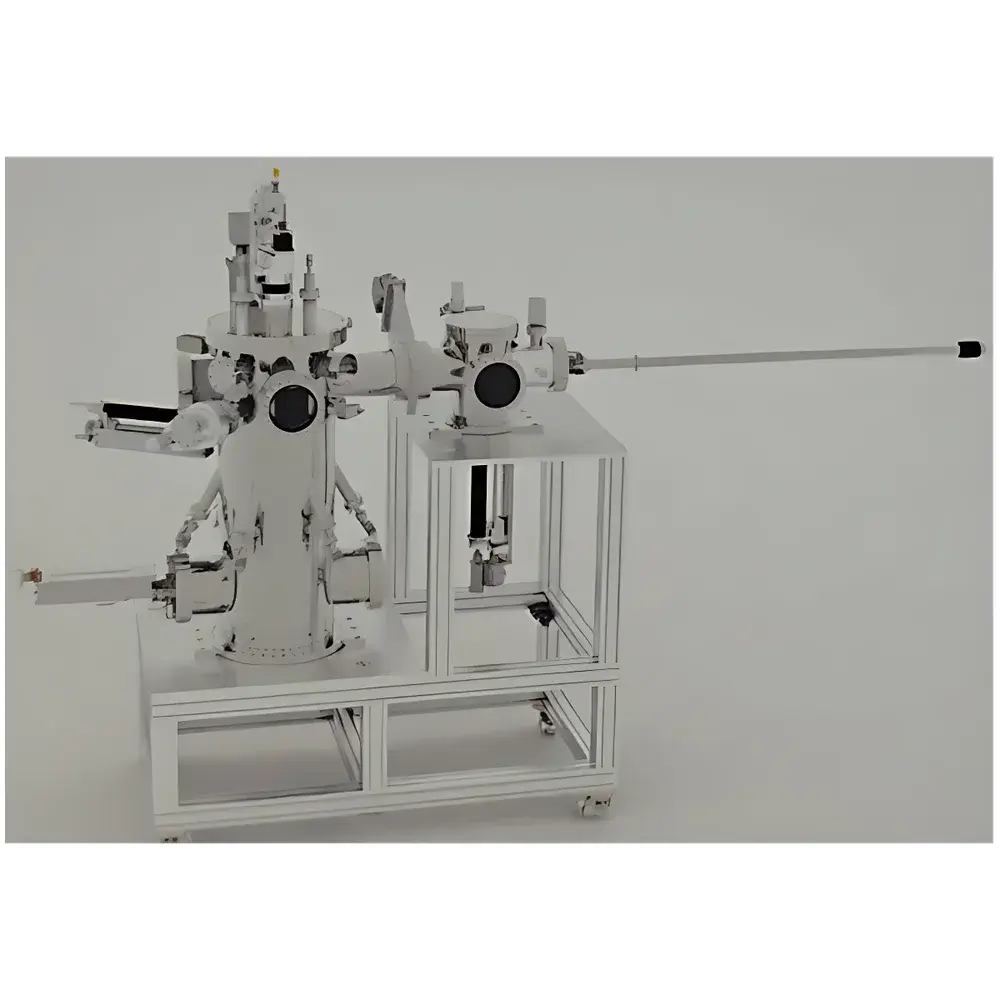
| Model | MBE-400 |
| Quotation | Upon Request |
| Substrate Heating | 2-inch Wafer Compatibility |
| Base Pressure | ≤1×10⁻¹⁰ mbar |
| Substrate Temperature Control | Room Temperature to 800 °C |
| Effusion Cell Sources | 6–10 Knudsen Cells |
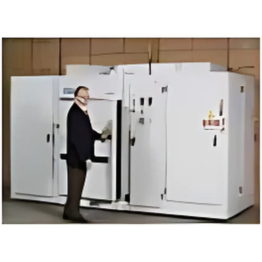
| Brand | MCC |
|---|---|
| Origin | USA |
| Manufacturer Type | Authorized Distributor |
| Product Category | Imported |
| Model | HPB-4 |
| Pricing | Available Upon Request |
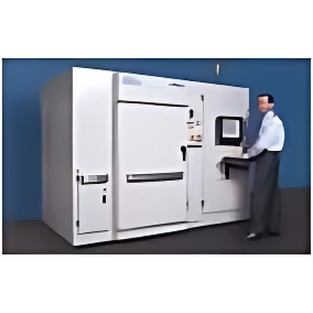
| Brand | MCC |
|---|---|
| Origin | USA |
| Manufacturer Type | Authorized Distributor |
| Origin Category | Imported |
| Model | HPB-5B |
| Pricing | Available Upon Request |
| Cooling Method | Forced Air with Precision Thermal Valves |
| Heating Mechanism | Integrated Heat-Sink Heaters |
| Max Power per DUT | 150 W |
| I/O Channels | 128 Independent |
| Vector Depth | Up to 32 M |
| Scan Memory | >1 GB |
| Repetition Rate | 10 MHz |
| Clock Speed | 400 MHz |
| Timing Resolution | 1 ns |
| Temperature Control | Per-DUT, Real-Time Monitoring & Closed-Loop Adjustment |
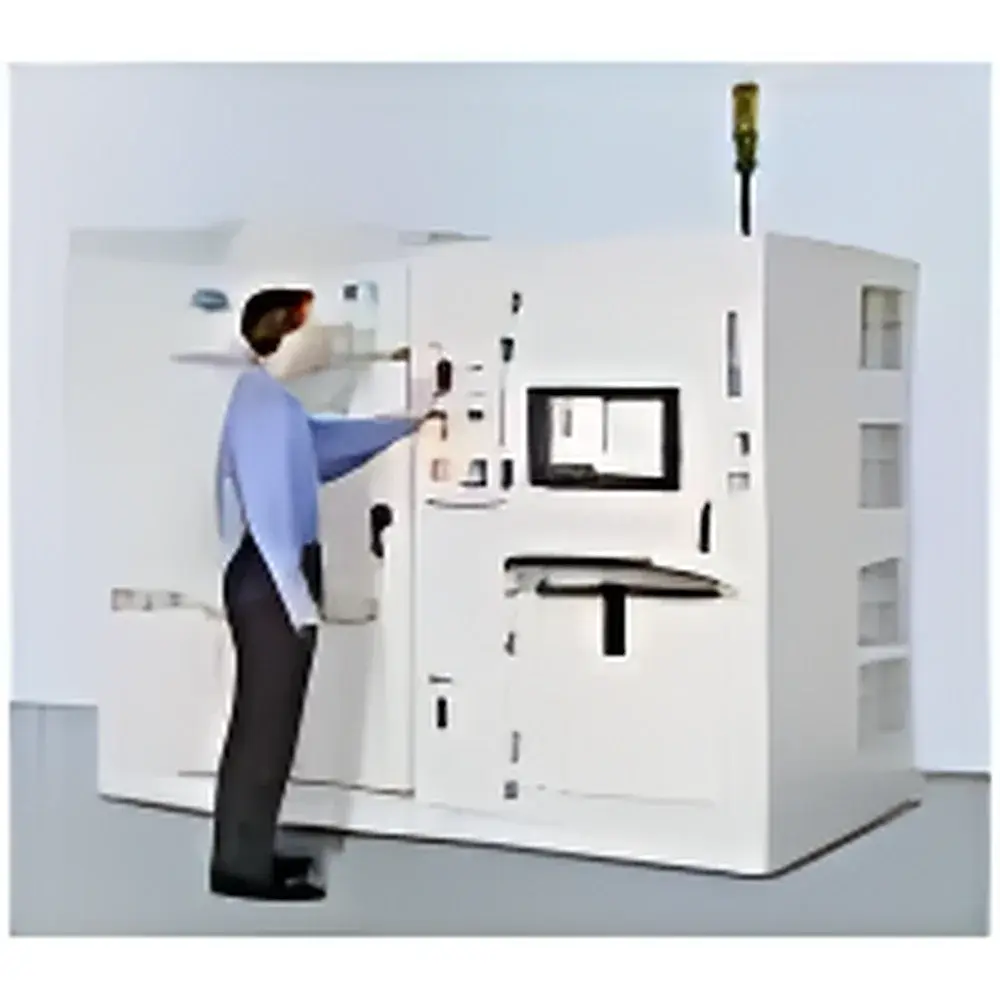
| Brand | MCC |
|---|---|
| Origin | USA |
| Manufacturer Type | Authorized Distributor |
| Origin Category | Imported |
| Model | LC-2 |
| Pricing | Upon Request |
| Board Dimensions | 317 mm × 609 mm (12.5″ × 24″) |
| Max Boards per System | 64 |
| Power per Board | Up to 400 W |
| Current per Board | Up to 240 A |
| I/O Channels | 128 independent |
| Vector Depth | Up to 4 M (upgradable) |
| Clock Resolution | 10 ns |
| Maximum Clock Frequency | 200 MHz |
| Max Device Power per Socket | 20 W |
| Concurrent Device Capacity | 1,536 devices |
| Thermal Control | Individual Chip Temperature Control (ICTC) via Pneumatic Cooling Valves and Heatsink-Based Resistive Heating |
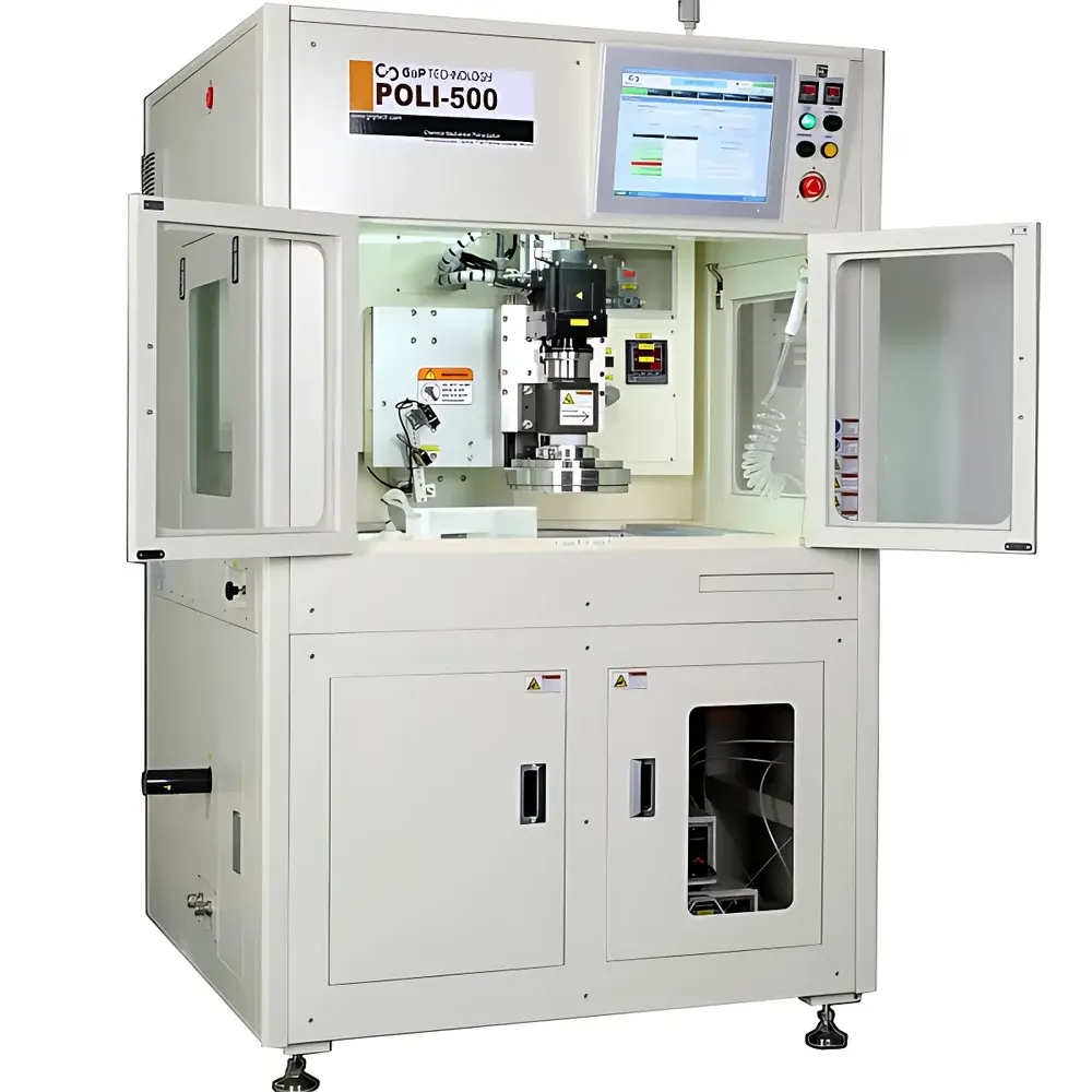
| Brand | MCF |
|---|---|
| Origin | Germany |
| Model | customized-17 |
| Platen Diameter | ≥508 mm (20 inch) |
| Platen Speed | 30–200 rpm |
| Wafer Pressure Range | 70–500 g/cm² |
| Retaining Ring Pressure Range | 70–700 g/cm² |
| Carrier Head Speed | 30–200 rpm |
| Oscillation Amplitude | ±10 mm |
| Slurry Delivery | 3-channel peristaltic pump system with adjustable flow and positionable nozzles |
| Endpoint Detection | Integrated friction force & infrared surface temperature monitoring |
| Control System | PC-based industrial controller with touchscreen HMI, 20 programmable recipes, up to 6 process stages per recipe |
| Within-Wafer Non-Uniformity (WIWNU, 1σ, EE=5 mm) | ≤5% |
| Wafer-to-Wafer Non-Uniformity (WTWNU) | ≤5% |
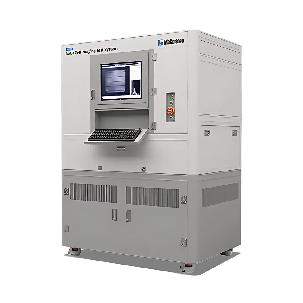
| Brand | McScience |
|---|---|
| Origin | Imported |
| Manufacturer Type | Authorized Distributor |
| Model | K3300PLX |
| Pricing | Available Upon Request |
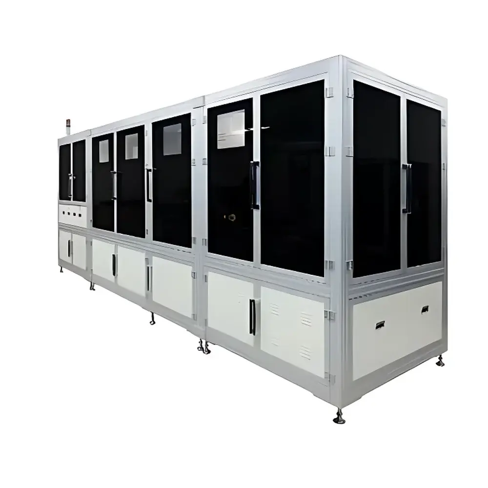
| Brand | McScience |
|---|---|
| Origin | South Korea |
| Model | K3500 |
| Application | In-line I-V characterization, electroluminescence (EL) / photoluminescence (PL) imaging, automated optical inspection (AOI), micro-crack & hot-spot detection |
| Compliance | Designed for ISO 9001-certified PV manufacturing environments |
| Control Interface | Touch-enabled HMI with recipe-based operation |
| Throughput | Up to 6,000 wafers/hour (standard 156.75 mm × 156.75 mm M2 cells) |
| Integration | Compatible with standard conveyor-based inline PV production lines (SECS/GEM optional) |
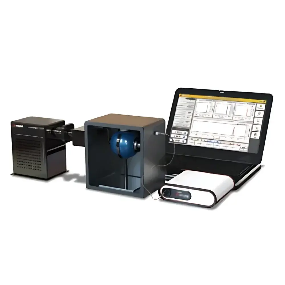
| Brand | McScience |
|---|---|
| Origin | South Korea |
| Model | L3000 |
| Type | Integrated PL/EQE/IQE/Spectral Characterization System |
| Sample Forms | Thin Films, Bulk Solids, Powders, Liquids |
| Measurement Modes | Steady-State PL, Time-Resolved PL (TRPL), External Quantum Efficiency (EQE), Internal Quantum Efficiency (IQE), Absorption Spectroscopy, Emission Spectroscopy |
| Excitation Sources | Tunable CW and Pulsed LEDs/Lasers (UV–Vis range) |
| Detection | Back-Thinned CCD or EMCCD Spectrometer (200–1100 nm) |
| Spectral Resolution | ≤ 0.1 nm (typ.) |
| Integration Time Range | 1 ms – 300 s |
| Software Control | Fully Automated via McScience PL-Studio v4.x |
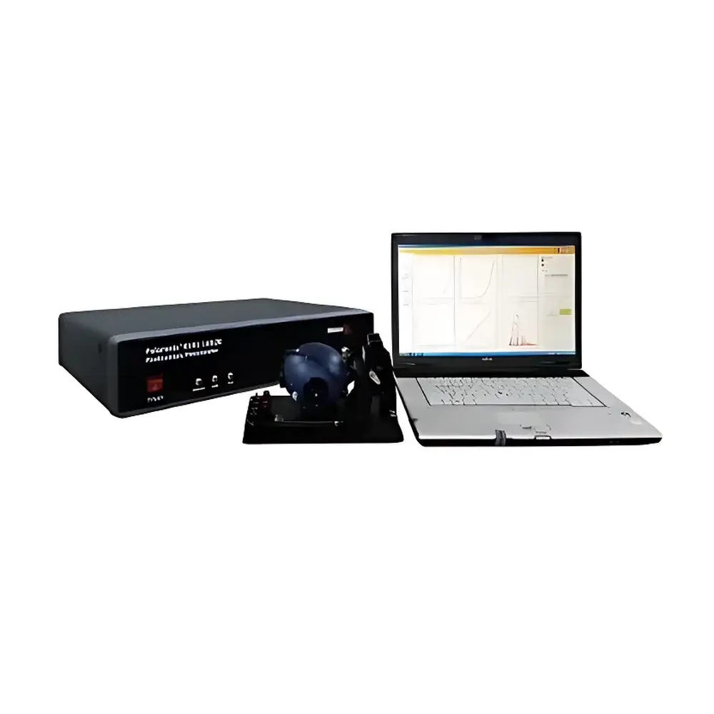
| Brand | McScience |
|---|---|
| Origin | South Korea |
| Model | L5300 |
| Type | Integrated PLQY & IVL Measurement Platform |
| Compliance | ISO/IEC 17025-aligned optical calibration traceability |
| Software | McScience QYLab v4.2 with audit trail and user access control |
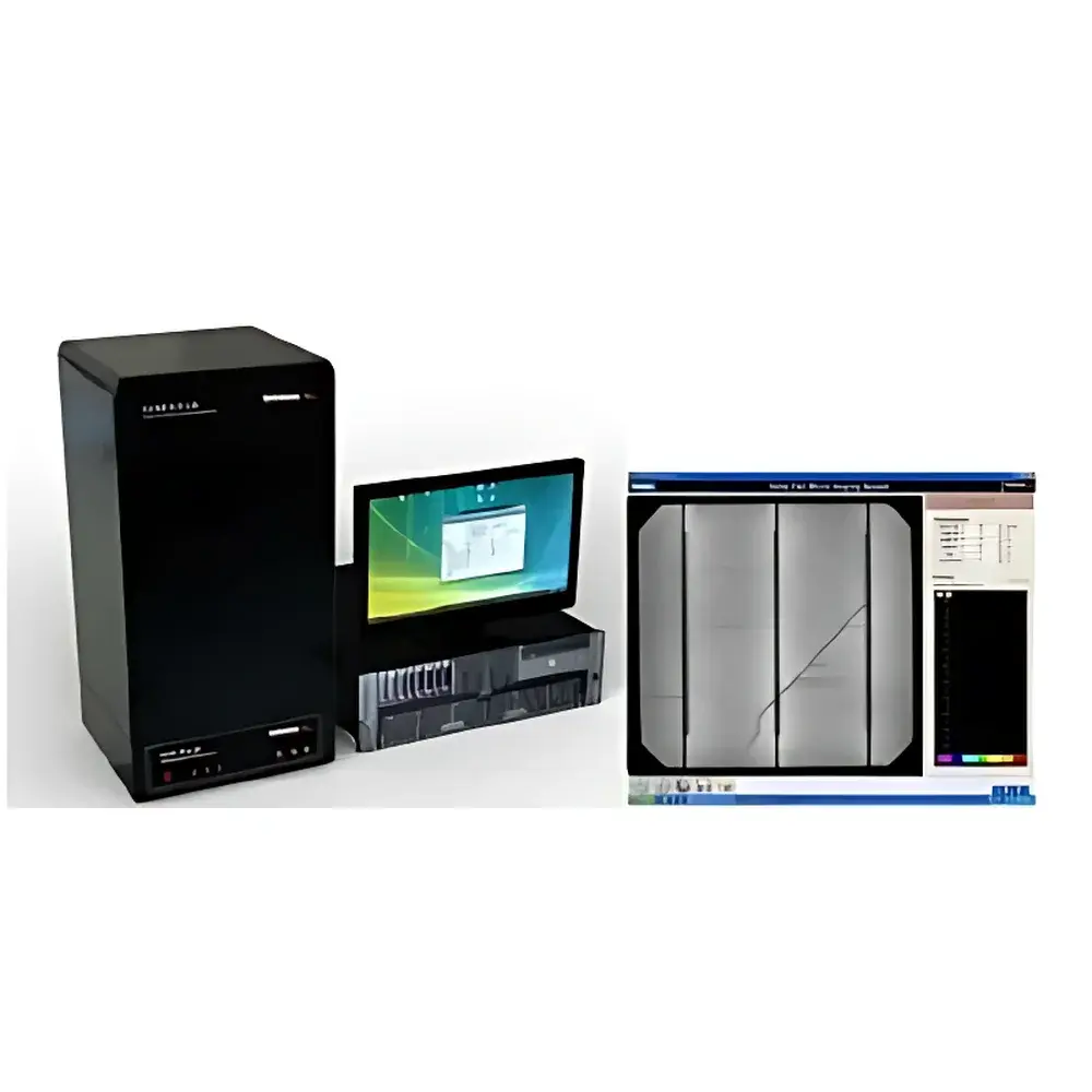
| Brand | McScience |
|---|---|
| Origin | Imported |
| Model | LAB |
| Power Supply | DC/Pulse |
| Operation Modes | Constant Current / Constant Voltage |
| Voltage Range | -20 V to +5 V |
| Current Options | 30 mA / 1 A / 20 A (user-selectable) |
| Imaging Sensor | High-Resolution CCD |
| Sample Compatibility | Individual Solar Cells & Large-Area PV Modules |
| Additional Capabilities | Integrated PL Imaging Option, Reflectance Mapping, LBIC (Light Beam Induced Current), Visual Inspection |
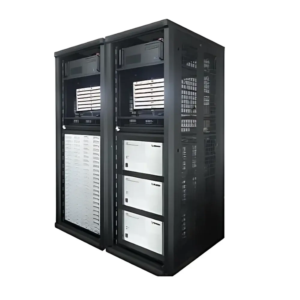
| Brand | McScience |
|---|---|
| Origin | South Korea |
| Manufacturer Type | Authorized Distributor |
| Origin Category | Imported |
| Model | M6000 |
| Pricing | Upon Request |